Communications and Network
Vol.11 No.04(2019), Article ID:95588,35 pages
10.4236/cn.2019.114007
Analysis of Wide-Bandgap Material OPFET UV Detectors for High Dynamic Range Imaging and Communication Applications
Jaya V. Gaitonde  , Rajesh B. Lohani
Department of Electronics and Telecommunication Engineering, Goa Engineering College, Goa University, Government of Goa, Ponda, India

Copyright © 2019 by author(s) and Scientific Research Publishing Inc.
This work is licensed under the Creative Commons Attribution International License (CC BY 4.0).
http://creativecommons.org/licenses/by/4.0/


Received: April 2, 2019; Accepted: October 7, 2019; Published: October 10, 2019
ABSTRACT
The ultraviolet (UV) photoresponses of Wurtzite GaN, ZnO, and 6H-SiC-based Optical Field Effect Transistor (OPFET) detectors are estimated with an in-depth analysis of the same considering the generalized model and the front-illuminated model for high resolution imaging and UV communication applications. The gate materials considered for the proposed study are gold (Au) and Indium-Tin-Oxide (ITO) for GaN, Au for SiC, and Au and silver dioxide (AgO2) for ZnO. The results indicate significant improvement in the Linear Dynamic Range (LDR) over the previously investigated GaN OPFET (buried-gate, front-illuminated and generalized) models with Au gate. The generalized model has superior dynamic range than the front-illuminated model. In terms of responsivity, all the models including buried-gate OPFET exhibit high and comparable photoresponses. Buried-gate devices on the whole, exhibit faster response than the surface gate models except in the AgO2-ZnO generalized OPFET model wherein the switching time is the lowest. The generalized model enables faster switching than the front-illuminated model. The switching times in all the cases are of the order of nanoseconds to picoseconds. The SiC generalized OPFET model shows the highest 3-dB bandwidths of 11.88 GHz, 36.2 GHz, and 364 GHz, and modest unity-gain cut-off frequencies of 4.62 GHz, 8.71 GHz, and 5.71 GHz at the optical power densities of 0.575 μW/cm2, 0.575 mW/cm2, and 0.575 W/cm2 respectively. These are in overall, the highest detection-cum-amplifi-cation bandwidths among all the investigated devices. The same device exhibits the highest LDR of 73.3 dB. The device performance is superior to most of the other existing detectors along with comparable LDR, thus, emerging as a high performance photodetector for imaging and communication applications. All the detectors show considerably high detectivities owing to the high responsivity values. The results have been analyzed by the photovoltaic and the photoconductive effects, and the series resistance effects and will aid in conducting further research. The results are in line with the experiments and the commercially available software simulations. The devices will greatly contribute towards single photon counting, high resolution imaging, and UV communication applications.
Keywords:
UV, OPFET, GaN, SiC, ZnO, Au, ITO, AgO2, High Dynamic Range, Imaging, Photon Counting, Communication

1. Introduction
This paper is an extension of work originally presented in 10th International Conference and Workshop (MULTICON-W 2019), International Conference on Trends in Electronics and Communications (TELCON) [1].
Ultraviolet (UV) photodetectors are useful in applications such as chemical, environmental, and biological analysis and monitoring, flame and radiation detection, astronomical studies, missile detection, and optical communication. UV high dynamic range imaging and single photon counting applications require photodetectors capable of resolving slight variations in light intensity without much compromising the responsivity, response time, bandwidth, and detectivity. On the other hand, UV communication requires photodetectors with high gain-bandwidth product with least compromising the other parameters. Wide-bandgap materials such as GaN, SiC, and ZnO open the door for UV detection and communication. The properties of semiconductor materials which decide their fate are the absorption coefficient, carrier lifetimes, saturation velocities, Schottky barrier height, and carrier mobilities. The external factors which influence the device performance incorporating these materials are the structural dimensions, doping concentration, optical power, operating wavelength, bias voltage, and the illumination model employed. Thus, the semiconductor properties along with the external factors, on the whole, determine the performance of the investigated device. The detectors are evaluated based on their performance metrics such as responsivity, gain, external quantum efficiency (EQE), sensitivity, switching time, bandwidth, LDR, detectivity, dark current, and unity-gain cut-off frequency. The devices that can function as photodetectors include p-n junction diodes, p-i-n diodes, avalanche photodiodes (APDs), metal-semiconductor-metal (MSM) photodiodes, Schottky barrier diodes, photomultiplier tubes (PMTs), phototransistors, photoFETs, heterostructure diodes, resonant cavity enhanced (RCE) photodiodes, nanostructured diodes, hybrid diodes, and travelling wave detectors. High dynamic range UV imaging and UV communication involve state-of-art photodetectors such as APDs and PMTs [2] [3] [4] [5]. However, APDs exhibit gain upto limited modulation frequencies after which the gain reduces significantly. PMTs offer high gain and bandwidth, but are bulky and fragile. To address these issues, a photo FET device viz. Optical Field Effect Transistor (OPFET) or optically-controlled Metal-Semiconductor Field Effect Transistor (MESFET) is suggested, which has so far delivered high gain and moderately high bandwidth [6] - [11]. The performance can be further improved through optimization. Several optimization procedures can be employed such as structural, material, illumination model, bias, wavelength, optical power, or a combination of the above.
In this paper, material, illumination model, and optical power-based optimization are adopted for enhancing the performance of the device towards high resolution UV imaging and UV communication applications. The materials chosen for this purpose are Wurtzite GaN, 6H-SiC, and ZnO. These materials have distinct electrical and optical properties which make the exploration of the devices incorporating these materials even more interesting. The work analyzes in-depth the performance of the OPFET UV detectors based on the material properties and external factors applied. The illumination models employed are the generalized model and the front-illuminated model. The gate materials being used are the gold (Au) and Indium-Tin-Oxide (ITO) for GaN, Au for SiC, and Au and silver dioxide (AgO2) for ZnO. The key changes of the present work with respect to the conference paper are that the original work only presented the performance evaluation and analysis of the generalized and the front-illuminated GaN OPFET models with Au gate and compared that to the previously published results on the GaN buried-gate OPFET models [12] towards high resolution UV imaging and UV communication applications. These devices could resolve subtle variations in light intensity better than the buried-gate devices and comparable to the reported literature [13] - [21] without much compromising the other detector parameters which were also superior to most of the existing detectors.
The characteristics of the detectors obtained depend largely on the photoconductive and the photovoltaic effects being developed limited by the voltage drop incurred across the series resistances. At certain instances, negative sensitivity is being observed i.e. increase in depletion width with illumination. Presence of traps largely slows down the response i.e. carrier lifetime is increased since significant amount of time is being spent on filling and emptying (trapping and de-trapping) of the carriers. However, this conversely increases the gain of the device since gain is directly proportional to the lifetime. On the other hand, illuminating the device can cause photoionization of the traps (i.e. release of carriers from traps) reducing the de-trapping time and hence, speeding up the response. But, photoionization does not fully compensate the effect of traps.
All the material properties depend upon the doping concentration. Hence, it determines the material properties to some extent as well as contributes to charge induced by doping, and in turn, the device current. Suppressing the dark current is an important aspect of the present technology. This enhances the photoresponse or photocurrent, improves the Signal-to-Noise ratio [22] and the device performance [23], enables high and low temperature operation [24], and allows functioning of detectors with standard CMOS readout circuits [23]. One way of suppressing the dark current is to employ a higher Schottky barrier height metal contact with the semiconductor. This decreases the depletion width, increases the series resistance, and lowers the current. Since the reverse saturation current density is inversely proportional to the barrier height, it is also significantly reduced. This, in turn, boosts the photovoltage, since the photovoltage is inversely proportional to the saturation current density. High Schottky barrier height also increases the depletion area for photogeneration and adds to the photoresponse. Employing a lower gate length also reduces the dark current. This can be explained as follows: The elongation of the gate length proportionally increases the active layer thickness and the gate width, and hence, the dark current. Depending upon the properties, each material may suit to a particular application better than the others. Thus, each material has its own significance.
This paper provides an in-depth analysis of SiC, GaN, and ZnO-based OPFET UV illumination models for high dynamic range imaging and communication applications. In GaN MESFET, due to the presence of deep traps, there is a current collapse under dark condition [25], due to the creation of depletion region, which reduces the current. However, the current is restored under sub-bandgap or bandgap illumination [26]. The deep electron traps do not alter the minority carrier (hole) lifetime in n-type material since electrons are in abundance but significantly modify and create long lifetimes of the majority carriers, since traps take significant time to trap and release the carriers. GaN is a direct bandgap material involving band-to-band radiative and Auger recombination processes. Hence, the hole lifetime in n-type GaN is of the order of 1 ns whereas the electron lifetime is of the order of 1 μs which is reflecting the value of majority carrier lifetime under illumination, lower than its value under dark, due to photoionization of traps under sub-bandgap or bandgap illumination. In 6H-SiC, there has been no evidence of electron and hole traps present in the material which is implanted with He+ ions. However, there are four significant recombination centres viz. Z1/Z2, S or E1/E2, R, and RD5 centres [27] [28]. These possess activation energies of 0.65 eV, 0.4 eV, 1.27 eV, and 0.43 eV respectively with respect to the conduction band. Since, SiC is an indirect bandgap material, the band-to-band radiative and Auger recombination processes contribute negligibly to the recombination lifetime. The only major recombination processes are through the involvement of traps. As such, the net recombination lifetime is of the order of 9.19 ns. The absence of electron or hole traps in the material results in equal majority and minority carrier lifetimes. In ZnO, which is a direct bandgap material, the major phenomena contributing to recombination are the band-to-band recombination processes. There has been observation of two electron traps in hydrothermal grown ZnO with activation energies of 0.22 eV and 0.47 eV with respect to the conduction band [29] which only alter the majority carrier electron lifetime in n-type material. As such, the minority carrier hole lifetime is of the order of 1 μs whereas the electron lifetime under dark condition is of the order of 0.176 ms. But, due to illumination, the electron traps are photoionized and results in release of carriers, thus, reducing the de-trapping time, and consequently reducing the lifetime of majority carriers i.e. the lifetime becomes around 1 μs at an optical power density of 0.575 W/cm2.
Although there has been significant research on MESFET-based photodetectors, optically-controlled amplifiers, oscillators, switches, and mixers, over the past few decades, the research focused on GaAs as the semiconductor which primarily operates in the visible to near-infrared region [6] - [11]. Hardly any research has been carried out on the UV responses of OPFET detectors. To the best of the authors’ knowledge, this is the first report and analysis of wide bandgap material-based OPFET UV detectors for communication and high dynamic range imaging applications.
The previous works on GaN-based buried-gate OPFET, generalized model of OPFET and front-illuminated OPFET UV detectors with Au gate showed excellent photoresponse, fast response times, high detectivity along with enhanced bandwidth [1] [12]. The sensitivity or dynamic range of the buried-gate OPFET was low down to 14 dB. This was improved using the front-illuminated model and the generalized model and was found to be 24 dB and 55 dB respectively. In this paper, further improvement in the linearity range upto 65 dB using different gate material (ITO) for GaN OPFET and upto 73 dB with other semiconductor materials (SiC, and ZnO) was achieved. Also, the bandwidth, response times, responsivity, and detectivity were greatly enhanced.
The rest of the paper is organized as follows: At first, a brief theory is presented followed by the results and discussion, and finally the conclusion of the work done.
2. Theory
The two models considered in this work (front-illuminated OPFET and generalized model of OPFET) are schematically shown in Figure 1 and Figure 2 respectively. In the 1st case, only the transparent gold (Au)/Indium-Tin-Oxide (ITO)/Silver dioxide (AgO2) gate is illuminated whereas in the 2nd case, the spacings between the gate and source, and the gate and drain are illuminated in addition to the gate area. The absorption of photons with energy greater than the bandgap of GaN in the regions below the gate (1st case and 2nd case) and the sidewalls of the gate depletion region (2nd case) creates electron-hole pairs in the respective regions. The photogenerated holes travel toward the junction while the electrons move toward the channel. A forward photovoltage is developed when the holes cross the junctions, reducing the depletion width and increasing the drain to source current (photovoltaic effect). On the other hand, the electrons move along the longitudinal area of the channel when the drain to source voltage is applied and contribute to the conductivity of the channel (photoconductive effect). The series resistances present in the area between the gate and source, and the gate and drain, limit the total current through voltage drops developed across these resistances. Thus, the photovoltaic and the photoconductive effects, and the series

Figure 1. Schematic of the front-illuminated OPFET.

Figure 2. Schematic of the generalized model of OPFET.
resistances effect can provide a complete explanation of the performance of these detectors.
In the practical devices, only the gate depletion region exists in the channel. The p-n junction depletion region extension in the channel ceases to exist owing to the combined effect of moderate channel doping concentration (5 × 10²²/m3) and low substrate impurity concentration (~1013/m3) substrate being semi-insulating. This also results in the complete depletion of the substrate region.
The space charge region extension in the channel measured from the surface is written as,
(1)
where Ndr is the doping concentration, ΦB is the Schottky barrier height, Δ is the position of Fermi level below the conduction band, ɛ is the permittivity of semiconductor, VOP1 is the photovoltage generated across the Schottky junction and v(x) is the channel voltage which varies from 0 at the source end to VDS at the drain end. VDS is the drain to source voltage and vgs is the gate to source voltage.
Photovoltage calculation in the front-illuminated OPFET model
In the gate depletion region, the hole continuity equation is written as
(2)
where p is the hole density, vy is the carrier saturated velocity, α is the absorption coefficient, Φ is the photon flux density, τωp is the hole lifetime under ac condition, and y is the distance from surface towards the substrate.
Its analytical solution is given as
(3)
where and , using the boundary condition at y = ydg,
.
The photovoltage is obtained as
(4)
where p(0) is the hole density computed at y = 0, Js1 is the reverse saturation current density across the Schottky junction, q is the electronic charge, k is the Boltzmann constant and T is the temperature.
Photovoltage calculation in the generalized OPFET model
To calculate the hole density in the sidewalls of the gate depletion region for the generalized model of OPFET, we define extension of the sidewall depletion regions in the channel as at the source end and at the drain end, where ydg0 is the value of ydg at v(x) = 0 and ydgV is the value of ydg at v(x) = VDs (assuming that the sidewalls are quarter arcs). xs is the linearly varying distance from 0 to ydg0 and xd varies linearly from 0 to ydgV. We can then calculate the hole density in the sidewalls at the source end, by substituting ydgs instead of ydg in the hole density equation (p(y)), and at the drain end, by substituting ydgd instead of ydg in the same equation (p(y)), thus giving hole densities, p2(y) and p3(y).
To calculate the photovoltage in the case of the generalized model of OPFET, we perform the following: We integrate p2(0) and p3(0) from 0 to xs and 0 to xd to give the number of holes per square metre crossing the junction, denoted by p21(0) and p31(0) respectively, by numerical integration using the Trapezoidal method. We can then write the photovoltage equation for the generalized OPFET model as:
(5)
where Z is the gate width and L is the gate length.
Photogenerated electron density calculation in the neutral channel region
The electron continuity equation in the channel region is expressed as
(6)
Here n is the electron density, Dn is the diffusion constant of electrons, τωn is the lifetime of electrons under ac condition.
The solution of Equation (8) obtained analytically is expressed as
(7)
where and , Lnω is the ac diffusion length of electrons, .
The boundary condition used is at y = 0,
Photogenerated electron density calculation in the depletion region
The continuity equation is represented by
(8)
Its solution is given as
(9)
Drain to source current calculation
The total conducting charge is expressed as,
(10)
Here Qd is the charge due to doping; Qch, Qdep1 and Qdep2 are the charges due to photogeneration in the channel, Schottky junction depletion region and the substrate depletion region respectively.
Then Qn can be evaluated as:
(11)
where nch, ndep1 and ndep2 are the photogenerated electron densities in the channel, Schottky junction depletion region and substrate depletion region respectively.
All the integrations concerned with the computation of charge are performed numerically using the Trapezoidal method.
The total drain to source current is then calculated using the model described in [30] :
(12)
The drain to source saturation current is calculated as:
(13)
where Qn(0) is the total conducting charge at the source end in the presence of series resistances.
η is the parameter giving the ratio of the drain-to-source conductance evaluated at VDS = 0 to the drain to source saturation current.
The drain to source conductance can be estimated as
(14)
where Gch is the channel conductance evaluated at VDS = 0 and is given by
(15)
Qn(0) is again the total conducting charge at the source end, however, in the absence of series resistances. Rs1 and Rd1 are the series source and drain resistances and Rsh is the drain to source shunt resistance.
The parasitic series source and drain resistances involved in the calculation are obtained following a similar procedure as given in [31]. The above current is applicable to the front-illuminated OPFET. In the case of the generalized model of the OPFET, the additional components of the current due to the contributions from the sidewalls of the gate depletion region are given as follows:
At the source end,
(16)
At the drain end,
(17)
Calculation of gate depletion region and sidewall space charge
The net space charge in the gate depletion region can be obtained as:
(18)
which is the difference between the doping-induced space charge and the photogenerated electron density in the depletion region since the photogenerated electrons deionize the space charge ions.
Similarly, the net space charge in the sidewalls of the gate depletion region is estimated as:
(19)
Thus, the total net space charge is:
(20)
The above calculation of the space charge is required for the estimation of the switching time.
Calculation of carrier lifetimes in the presence of traps
The SRH (Schockley Read Hall) recombination lifetime of carriers in the presence of traps is given by [32] :
(21)
where the symbols have the same meaning as in [32].
The definitions of various detector parameters along with their equations are presented in Table 1 from which the necessary concurrences and interrelationships can be derived.
3. Results and Discussion
The simulations have been performed using MATLAB Software with MEX coding feature. We set the gate-source voltage to 0 V and the drain-to-source voltage to 10 V (saturation region). The wavelength of operation is 350 nm. This UV wavelength falls in the range of UV Type A radiation (315 - 400 nm) which is least harmful to the humans and accounts for 95% of the sun’s radiation reaching the earth’s surface. However, there is some risk of damage caused by this type of radiation, hence, preventive measures need to be taken. The other UV ranges (Type B (280 - 315 nm)) and Type C (100 - 280 nm) are significantly damaging and hence, should be avoided. The photon flux densities used in the simulations (1016, 1019, and 1022/m2-s) correspond to optical power densities of 0.575 μW/cm2, 0.575 mW/cm2, and 0.575 W/cm2 respectively. The performance evaluation of the GaN, SiC, and ZnO-based illumination OPFET models considered in this work (generalized model and front-illuminated model) with respect to the performance metrics along with the previous work results [1] [12] is provided in Table 2. The comparison of our simulations with the reported work is presented in Table 3. The parameters employed in calculation are listed in Table 4. Figure 3 shows the validation of the present model with the experimental results given in [6] portraying close resemblance. The results have been compared with the commercially available software (Visual TCAD)-based simulations and have shown close match (Figures 4-7). Figure 8 presents the drain to source current-voltage characteristics for the ITO-gated generalized model of GaN OPFET device at different flux densities showing the clear sensitivity to optical illumination. Figure 9 demonstrates the frequency response of the device at different flux densities indicating the bandwidth dependence upon flux.
The performance and the analysis of the buried-gate, generalized, and front-illuminated GaN OPFET models with Au gate has already been presented in [1] [12]. The results are repeated here in Table 2 along with the present simulation results for comparison. In this paper, an in-depth discussion of the
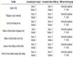
Table 1. Various detector parameters.
Table 2. Performance comparison of GaN, SiC, and ZnO OPFET illumination models.
Table 3. The comparison of simulations with the literature.
Table 4. Parameters used in calculation.

Figure 3. Comparison of the present model results with the experiments [6].

Figure 4. Comparison of the present model results with the simulations using Visual TCAD software (Au-GaN front-illuminated OPFET).

Figure 5. Comparison of the present model results with Visual TCAD (Au-SiC front-illuminated OPFET).

Figure 6. Comparison of the present model results with Visual TCAD (Au-ZnO front-illuminated OPFET).

Figure 7. Comparison of the present model results with Visual TCAD (Au-SiC generalized model of OPFET).

Figure 8. Drain to source current-voltage characteristics of the ITO-gated GaN generalized OPFET device.

Figure 9. Frequency responses of the ITO-gated generalized GaN OPFET device.
performance of the investigated devices and the relative comparison, analysis with the devices previously studied will be provided. The superiority of the investigated devices with respect to the performance metrics over other detectors and comparable LDR values are clearly depicted from Table 2 and Table 3.
Note that the unit of detectivity wherever mentioned in the results and discussion i.e. Jones corresponds to cmHz1/2W−1.
Beginning the discussion with 6H-SiC OPFET considering the generalized model, it was found that this device exhibits very high photovoltages (2.22 V, 2.76 V, and 3.3 V) at the flux densities of 1016, 1019, and 1022/m2-s respectively. This is attributed to the large Schottky barrier height of the Au-SiC contact (1.37 eV) which effectively reduces the reverse saturation current density across the Schottky junction and in turn, boosts the photovoltage since the photovoltage is inversely related to the saturation current density. This effect is assisted by the significant saturated hole velocity (9 × 10⁴ m/s) since photovoltage is directly related to the saturated velocity. Although SiC possesses moderately low absorption coefficient (1.06 × 10⁵/m) and low hole lifetime (9.19 ns) upon which the photogenerated hole density is directly dependent and which tend to reduce the photovoltage, the supporting effects greatly supersede the limiting effects resulting in very high photovoltages. One more reason for the developed photovoltages is owing to the contributions of the photogenerated hole density from the sidewalls of the gate depletion region in addition to the gate depletion region itself. The large barrier height also greatly reduces the dark current by rendering the channel width to zero and substantially raises the series resistances. The dark current contribution from the channel is zero and a small current flows owing to the contribution from the shunt resistance. Under illumination, the series resistances are considerably reduced due to very high photovoltages. Thus, on account of the very high photovoltages and low dark current, the photocurrents generated are high (3 mA, 3.8 mA, and 4.5 mA). The sensitivity is very large at the lower flux density (96.8%) due to large photocurrent and very low dark current. However, as the flux density is increased, the current involved is larger but is limited by the voltage drop incurred across the series resistances, hence, the sensitivity falls at the higher intensities (19.7% and 16.3%) assisted by the fact that the device current is not significantly higher as compared to that at the previous flux density. The transconductances attained are (0 mS, 1.7 mS, 1.5 mS, and 1.1 mS). The transconductance ought to have increased with illumination explained by the fact that at a fixed doping concentration, the depletion width sensitivity to the applied gate-to-source voltage is larger at higher photovoltages. But, the series resistance limits the said sensitivity at higher flux densities leading to a fall in the transconductance with illumination. It will be worth mentioning here that the drain-to-source conductance evaluated as drain-to-source voltage tends to zero is almost insensitive to the change in the flux density (0.08 mS, 0.87 mS, 0.88 mS, 0.88 mS) since zero drain-to-source voltage means zero drain-to-source current which incurs no voltage drop across the series resistance. In other words, it means that the channel charge is calculated in the absence of series resistances. Thus, the conducting charge at the source end of the device upon which the conductance depends is almost the same at all the three flux densities since the large photovoltages render the depletion width to zero and maintain constant channel charge. This charge determines the internal conductance. However, the external conductance is limited by the series resistances but is insensitive to illumination due to lesser variation in the series resistances. This effect would have affected and limited the transconductance (due to the zero depletion width making it insensitive to the applied gate-to-source voltage) through the parameter eta (η) which is the ratio of the said conductance to the drain-to-source saturation current under the hyperbolic tangent expression in the drain-to-source current equation if the device was biased in the linear region of operation. However, in the present case, since the device is biased in the saturation region of operation, this effect is evaded. The gate-to-source capacitances achieved are (0 pF, 0.06 pF, 0.028 pF, 0.031 pF). Again, the capacitance ought to have increased with illumination, however, owing to the same reason (depletion width sensitivity) as in the case of the transconductance there is a fall in the capacitance initially and then remains almost constant. As such, the unity-gain cut-off frequencies attained are (0 GHz, 4.62 GHz, 8.71 GHz, and 5.71 GHz). The obtained high 3-dB bandwidths of (11.88 GHz, 36.2 GHz, and 364 GHz) have been attributed to the very high photovoltaic effect and the short hole lifetime (9.19 ns) with the photoconductive effect contributing negligibly to the response due to the short electron lifetime (9.19 ns) which tend to reduce the bandwidth when it is comparable to the photovoltaic effect. The bandwidth rises with illumination as the photovoltage is boosted with the increase in the optical power. This can be explained as follows: The fact that the depletion width sensitivity is increased at higher photovoltages is translated in the form of roll-off slope of the frequency response curve to be gentler as the flux density increases thus, widening the response and incrementing the bandwidth. The series resistance although limits the sensitivity at dc or low frequencies, as the frequency increases, the current significantly drops which reduces the effect of series resistance and allows the device to utilize the full potential of the available sensitivity at or near the 3-dB point. The response or the switching times are as (4 ns, 79 ps, 57 ps, and 43 ps). The value under dark is comparatively large owing to the complete depletion of the channel due to large barrier height which induces maximum space charge under the gate and its sidewalls and the low dark current which altogether increase the switching time, switching time being given by the ratio of the space charge to the drain-to-source current. Under illumination, there is a significant improvement in the response time owing to the large photovoltaic effect which induces high currents and the same simultaneously decreasing the space charge through a reduction in the depletion width. The photoconductive effect does not play any role at any of the flux densities since the short electron lifetime makes it negligible compared to the photovoltaic current. On account of the high photovolatges, the responsivities attained are high (1.56 × 10⁹ A/W, 2 × 10⁶ A/W, and 2.35 × 10³ A/W). The photocurrent gain and the external quantum efficiency (EQE) are also high which follow a similar explanation since they are strongly dependent on the photocurrent as the responsivity does. The drain-to-source resistance, Rds and the channel conductance, gd which are the reciprocals of one another significantly decrease (103 kΩ, 40.97 kΩ, 18.26 kΩ, and 9.28 kΩ) and increase (0.0097 mS, 0.024 mS, 0.055 mS, and 0.11 mS) with illumination since although the drain-to-source conductance is insensitive to illumination, the saturation current increases significantly with the optical power and it has been observed that the value of hyperbolic tangent expression is more sensitive to the applied drain-to-source voltage when the saturation current is higher. The drain to source resistance, source and drain series resistances, and various other resistances (gate bias resistance, load resistance, input resistance, and the drain resistance) are useful in determining the noise current. The noise current also depends upon the absolute temperature and the 3-dB bandwidth. Higher the bandwidth, higher the noise current and the noise current is inversely proportional to the resistances. Since the drain-to-source resistance and the series resistances decrease with illumination and the bandwidth increases with illumination, the noise current increases with optical power (0.75 pA, 2.31 pA, and 23.6 pA). The noise equivalent power (NEP) is given by the ratio of the mean squared noise current to the responsivity. Due to a significant decrease of responsivity by three orders of magnitude with periodic increase in the intensity, the NEP considerably increases with the optical power (0.55 fW, 0.78 pW, and 2.1 nW). The parameter detectivity which depicts the ability to detect weak signals in the presence of noise is expressed as the ratio of the square root of the product of detector area and the bandwidth to the noise equivalent power. Although the bandwidth rises with illumination, the effect of periodic increase in NEP is felt more resulting in a periodic decrease in detectivity (3.4 × 10¹⁷ Jones, 4.2 × 10¹⁴ Jones, and 5 × 10¹¹ Jones). The detectivities are high due to high responsivities. The SiC OPFET device exhibits a large LDR of 73 dB owing to its low dark current and high photocurrent.
ZnO is a known for its high absorption coefficient (2.7 × 10⁷/m), long carrier lifetimes (1 μs) (in the present work), and high hole saturation velocity (1.8 × 10⁵ m/s). This tends to increase the photovoltage developed in ZnO OPFET (generalized model) even higher as compared to that in SiC OPFET device but its low barrier height with the Au metal (0.65 eV) pegs its little back in developing the said photovoltage. Nevertheless, it generates considerably high photovolatges (1.616 V, 2.15 V, and 2.67 V). The contribution from the sidewalls of the gate depletion region also adds to the response. The dark series resistances are substantially lower than that in SiC OPFET owing to the lower barrier height. Under illumination, the resistances are significantly reduced but are comparatively higher than that in SiC OPFET due to lower photovoltages. Also, the dark current is substantially higher owing to the lower barrier height (0.425 mA). Although the photovoltages developed are lesser as compared to that in the SiC OPFET producing lesser photovoltaic charge, the ZnO device contributes significantly to the response (3.1 mA, 3.8 mA, and 8.1 mA). This is ascribed to the higher electron saturation velocity (2.8 × 10⁵ m/s) of ZnO in contrast with that of SiC (2 × 10⁵ m/s) upon which the saturation current depends. In contrary to the SiC device, the ZnO OPFET exhibits large photoconductive effect at the flux density of 1022/m2-s. This has been enabled by the high absorption coefficient of ZnO and the long electron lifetime which directly boosts the photoconductive effect. It has been observed that the device exhibits negative sensitivity at this intensity. This is because, the large photoconductivity develops high current which develops significantly high voltage drop across the series resistance reducing the channel width to zero by superseding the effect of high photovoltage at this intensity. In this case, the saturation current grows without bounds since the photoconductive effect is independent of the depletion width and reaches a large value. The drain-to-source conductance being evaluated at VDS = 0, the zero depletion width due to the high photovoltage results in high photovoltaic charge which is higher than the photoconductive contribution from the neutral channel region which ought to have produced substantially high conductance but due to the lower electron mobility of ZnO (320 cm2/(V∙s)) and significant series resistances limits the conductance to 0.8 mS at this intensity. The high saturation current has both an enhancing as well as a limiting effect (through the ratio of conductance and saturation current (parameter η) in the hyperbolic tangent expression) which along with a moderate conductance results in a high drain-to-source current (8.1 mA). The conductance remains almost insensitive to the change in flux density (0.28 mS, 0.796 mS, 0.8 mS, and 0.8 mS) due to the reasons stated earlier. The sensitivities attained are (85.9%, 19.2%, and 52.9%). At the intensity of 1016/m2-s, the high sensitivity is owing to high photocurrent. As the flux density is increased to 1019/m2-s, the sensitivity drops to 19.2% owing to the effect of the series resistance as well as the device current at this intensity is not significantly enhanced as compared to that at the previous flux density. The increase in sensitivity at the flux density of 1022/m2-s is due to the large photoconductive effect. The ZnO OPFET shows response times of (0.837 ns, 77.3 ps, 56.7 ps, and 7.8 ps). The considerably lower switching time under dark as compared to that in SiC (4 ns) is attributed to the lower barrier height which reduces the space charge and due to the higher dark current. With the device illuminated, the switching times are nearly the same in both the ZnO and the SiC devices at the lower intensities since the higher barrier height in SiC is compensated by the higher photovoltage and the lower photovoltage in ZnO is compensated by the lower barrier height resulting in almost equal currents and space charges assisted by the higher electron saturation velocity in ZnO. However, at the flux density of 1022/m2-s, there is significant improvement in the response time in ZnO OPFET (7.8 ps) as compared to that in SiC OPFET (43 ps) owing to the large photoconductive electron densities reducing the space charge in the depletion region in addition to increasing the current in ZnO device whereas the photoconductive current is negligible as compared to the photovoltaic effect in SiC OPFET. The transconductances observed are (1 mS, 1.7 mS, 1.5 mS, and 25.5 μs). The finite transconductance in the ZnO OPEFT under dark (1 mS) as opposed to the zero transconductance in the SiC OPFET is due to the finite channel width in ZnO OPFET owing to the lower barrier height whereas the SiC OPFET is completely and deeply depleted on account of the high barrier height which fails to register any change with the applied gate-to-source voltage. The equal transconductances under illumination at the lower intensities is due to the compensation mechanism of the barrier height and the photovoltage as discussed earlier along with the higher electron saturation velocity in ZnO and these decrease with illumination due to the voltage drop induced across the series resistance. The significant fall in the transconductance in ZnO OPFET device at the intensity of 1022/m2-s is owing to the complete depletion of the channel resulting in the insensitivity of the saturation current to the applied gate-to-source voltage whereas the conductance remains almost unaltered due to the large photovoltage maintaining zero depletion width. The gate-to-source capacitances estimated are (0.06 pF, 0.05 pF, 0.033 pF, and 7.43 fF). These are near to that in SiC OPFET at the lower intensities due to the compensation effects previously discussed. At these intensities, the capacitance falls with the increase in optical power due to the effect of series resistance. At the higher intensity, the capacitance falls as compared to that in SiC OPFET device and also with respect to the lower flux densities since the large photoconductive effect in the depletion region neutralizes the charged donor ions in the space charge region at this intensity in addition to the complete depletion of the channel which restricts the sensitivity of the depletion width to the applied gate-to-source voltage. Thus, the fT values achieved are (2.72 GHz, 5.38 GHz, 7 GHz, and 0.546 GHz). The long carrier lifetimes in ZnO result in 3-dB bandwidths of (38.6 MHz, 0.13 GHz, and 3.84 MHz) as opposed to that in SiC OPFET (11.88 GHz, 36.2 GHz, and 364 GHz) since bandwidth is inversely proportional to the lifetime. At the lower intensities, only the large photovoltaic effect contributes. The bandwidth increases with illumination due to the enhancement of the photovoltaic effect which makes the roll-off slope of the frequency response curve gentler as discussed earlier. At the higher intensity, the bandwidth falls due to the following: In this case, under dc conditions or at low frequencies, only the large photoconductive effect contributes. But, as the modulation frequency is increased, the photoconductive current reduces which opens the channel wide enough from the fully depleted state as a result of reduced voltage drop across the series resistance, thus, at or near the 3-dB point, both the photovoltaic and photoconductive effects contribute significantly and comparably. It is noted from self-analysis that when two independent phenomena with almost equal or comparable magnitudes and almost equal frequency responses emanating from equal carrier lifetimes are added to each other, the resulting net frequency response has a bandwidth which is lower than that of the independent processes. Since both the photoconductive and the photovoltaic effects have comparable magnitudes with equal electron and hole lifetimes, the net frequency response is narrower with respect to the individual responses resulting in a fall in the bandwidth (3.84 MHz). The responsivities are high (1.38 × 10⁹ A/W, 1.8 × 10⁶ A/W, and 4 × 10³ A/W) due to high photovoltaic effect and the photoconductive effects at the respective intensities. These are slightly lower than that in the SiC OPFET at the lower intensities due to lower photovoltages and higher at the flux density of 1022/m2-s due to the significantly high contribution from the photoconductive effect. The photocurrent gains and the quantum efficiencies are also high. The drain-to-source resistance and the channel conductance both significantly decrease (103 kΩ, 32 kΩ, 14.4 kΩ, and 1.25 kΩ) and increase (0.0097 mS, 0.031 mS, 0.069 mS, and 0.8 mS) with illumination owing to the same reasons as described earlier for SiC OPFET. However, at the intensity of 1022/m2-s, there is a considerable enhancement of conductance since at this intensity, the saturation current is independent of the depletion width sensitivity due to complete depletion of the channel owing to large photoconductive effect and hence, the saturation current increases without bounds which results in linear relationship between current and voltage even at high voltages enhancing the conductance. The noise currents in the ZnO OPFET are comparatively lower than that in the SiC OPFET owing to the lower bandwidths (2.24 fA, 7.68 fA, and 0.274 fA). This results in lower NEPs since the responsivities are either comparable or significantly higher (0.0345 fW, 0.05 pW, and 4.4 pW). But, due to the effect of lower bandwidths at the lower intensities, the detectivity is slightly lower in ZnO OPFET (3.12 × 10¹⁷ Jones, and 3.9 × 10¹⁴ Jones). At the higher intensity, the detectivity is considerably enhanced owing to both lower noise current and higher responsivity leading to much lower NEP superseding the effect of lower bandwidth (7.74 × 10¹¹ Jones). In the ZnO OPFET, the large depletion thickness in the substrate region (0.75 μm) ought to have produced high photoconductive effect but since the absorption coefficient of ZnO is high (2.7 × 10⁷/m) corresponding to an absorption depth of 0.037 μm, only the channel experiences significant photogeneration whereas the carriers are severely degraded upon reaching the substrate region due to the exponential dependence of the generation rate on the distance. The LDR exhibited by the device is moderately high (41 dB) owing to the large photocurrent but higher dark current.
In the SiC OPFET considering the front-illuminated model, the photovoltages developed are lower (0.79 V, 0.97 V, and 1.15 V) due to the contributions only from the gate depletion region. Hence, the series resistances are comparatively higher. The dark current is the same due to the same structure (surface gate). Under illumination, the drain-to-source currents are lower owing to the lesser photovoltages. The sensitivities attained are (81.12%, 33.3%, and 33.18%). The high sensitivity at the lower intensity is due to the significant photocurrent and the low dark current. With the increase in the flux density, the sensitivity drops to moderate 33.3% and remains 33% at the higher intensity, since the enhancement of photocurrent with respect to the previous flux density is not significantly high. The response times in the front-illuminated model are higher as compared to that in the generalized model (0.7 ns, 0.4 ns, and 0.288 ns) due to the lower currents involved and higher space charges on account of the lesser photovoltages. The transconductances (0 mS, 1.2 mS, 1.7 mS, and 3 mS) and the gate-to-source capacitances (0 pF, 0.0658 pF, 0.0836 pF, and 0.113 pF) in the front-illuminated model exhibit their normal behavior of periodically rising values with the increase in the intensity due to the usual fact that the depletion width sensitivity increases at the higher photovoltages since in this case, the sensitivity is not limited by the voltage drop across the series resistance owing to the currents involved being lower. Hence, the unity-gain cut-off frequencies obtained are (0 GHz, 2.87 GHz, 3.25 GHz, and 4.18 GHz). It is noticed that the drain-to-source conductance significantly varies with illumination (0.0616 mS, 0.366 mS, 0.46 mS, and 0.59 mS) as opposed to the insensitivity observed in the generalized model. This is because, here, the photovoltages developed are considerably lower which maintain finite depletion width thus, clearly showing the contrast in the sensitivities and the conductance is less affected by the series resistances due to the lower charges involved. The 3-dB bandwidths are substantially lower (1.625 GHz, 3.1 GHz, and 2.42 GHz) than that in the generalized model due to the inferior photovoltaic effect. This effect also reduces the responsivity (2.39 × 10⁸ A/W, 3.9 × 10⁵ A/W, and 6.048 × 10² A/W), the gain, and the EQE. The drain-to-source resistance (103 kΩ, 103 kΩ, 103 kΩ, and 102.3 kΩ) and the channel conductance (9.71 μS, 9.71 μS, 9.71 μS, and 9.77 μS) are insensitive to illumination due to the lower currents involved as discussed earlier. The noise currents are greatly reduced owing to the narrower bandwidths (0.0463 pA, 0.11 pA, and 0.105 pA). The corresponding NEPs are (0.9 fW, 0.85 pW, and 0.536 nW) which are larger than that in generalized model at the lower intensities due to the inferior responsivities but reduced at the higher intensity, since in this case, the effect of higher noise current due to large bandwidth (364 GHz) in the generalized model is felt more than the effect of lower responsivity in the front-illuminated model. As such, the detectivities obtained are (7.75 × 10¹⁶ Jones, 1.13 × 10¹⁴ Jones, and 1.59 × 10¹¹ Jones). A moderate LDR of 41.4 dB is achieved owing to the low dark current and significant photocurrent.
The overall performance of the ZnO OPFET detector considering the front-illuminated model falls with respect to the generalized model since excluding the illumination in the spacings of gate and drain/source restricts the photovoltaic contribution to the gate depletion region only resulting in lesser photovoltages (0.58 V, 0.76 V, and 0.93 V). Hence, the drain-to-source currents obtained are significantly lower (1.6 mA, 1.9 mA) at the intensities of 1016 and 1019/m2-s whereas these are slightly lower (7.8 mA) at the flux density of 1022/m2-s, since at this intensity, the current is independent of the photovoltaic effect owing to the negative sensitivity resulting from large photoconductive effect which completely depletes the channel and since the channel thickness is the same in both the cases, the photoconductive contribution from the gate depletion region is the same. However, the slight difference in currents is attributed to the exclusion of the photoconductive effect from the sidewalls of the gate depletion region in the case of the front-illuminated model. In addition, although the saturation current is unaltered, and the internal drain-to-source conductance is the same owing to equal channel charges resulting from the developed photovoltage rendering the depletion width to zero in both the cases, there is slight reduction in the drain-to-source conductance emanating from the higher series resistances in the front-illuminated model which restricts the external conductance. It is worth noting here that in spite of the device biased in the saturation region, the drain-to-source current depends upon the conductance. This can be explained by the fact that at this intensity, the saturation current has increased to a large value without bounds since the channel is totally depleted owing to large photoconductivity and the depletion width sensitivity has no role to play in this case. Since the saturation current is large, it acts as a limiting factor (through the parameter η as discussed earlier) and this results in the current dependence upon the conductance. However, these currents and the photocurrents are considerably enhanced as compared to that in the SiC OPFET. This is due to the higher electron saturation velocity in ZnO and the lower barrier height of Au-ZnO junction inducing more channel charge surpassing the effect of lower photovoltages at the lower intensities and significantly high photoconductivity in the ZnO OPFET as compared to negligible photoconductivity in the SiC OPFET at the higher intensity. The sensitivities exhibited by the device are (72.2%, 17.97%, and 75.64%). The drop in sensitivity at the moderate intensity is owing to the series resistance limiting effect as well as the lesser enhancement of photocurrent with respect to the previous flux density. The switching times are degraded (0.197 ns, and 0.15 ns) as compared to the generalized model at the lower intensities owing to the lesser photovoltages which reduce the currents as well as enhance the space charges whereas there is slight change in the response time at the higher intensity (11 ps) due to almost same photoconductive effect. Despite of the inferiority of the front-illuminated model of ZnO OPFET device realized so far, there is a significant improvement in the transconductance (2.8 mS, 1.9 mS, and 0.864 mS). This emanates from the reduced effect of series resistance at the lower intensities due to the currents involved being lower which allows the device to substantially explore the available sensitivity. At the higher intensity, the improvement is owing to the following: the saturation current is large and the same in both the cases, but it is insensitive to the applied gate-to-source voltage due to completely depleted channel as discussed earlier. The large saturation current which acts as a limiting factor allows the conductance to decide the value of the net current. In both the cases, the internal conductance is largely insensitive to the applied gate-to-source voltage since the large photovoltage renders the depletion width to zero leading to significantly reduced transconductance. However, in the front-illuminated model, it has been observed that the series resistances undergo greater change with the variation in the gate-to-source voltage. This in turn, results in larger variation in the external conductance as compared to the generalized model comparably improving the transconductance. The fall in the transconductance from 2.8 mS to 1.9 mS as the flux density is varied from 1016/m2-s to 1019/m2-s is owing to the effect of series resistance. The gate-to-source capacitance first increases with the increase in flux density from dark to 1016/m2-s (0.06 pF, and 0.14 pF) due to the photovoltaic sensitivity and then decreases with the further increment in the optical power (0.0891 pF, and 0.0175 pF) owing to the limitation by the series resistance as well as due to the photoconductive effect neutralizing the space charges especially at the flux density of 1022/m2-s, the photoconductive effect being comparable to the doping induced space charge as a result of the high absorption coefficient of ZnO and the long electron lifetime. These transconductance and the capacitance values result in the fT values of (3.256 GHz, 3.346 GHz, and 7.86 GHz) which are inferior to both SiC OPFET and ZnO OPFET considering the generalized model at the lower intensities since although there is substantial improvement in transconductance, the capacitance is also increased by a similar factor and are comparable to the SiC OPFET (front-illuminated model) since similar scenarios exist in this case. Whereas at the higher intensity, the fT is superior to all the other cases, since in ZnO OPFET (generalized model) even though the photoconductive effect is comparable which reduces the space charges, the transconductance has substantially reduced and in SiC OPFET models, the photoconductive effect is negligible which maintains higher capacitance.
The drain-to-source conductance shows sensitivity to illumination as the intensity is raised from dark to 1016/m2-s (0.278 mS, and 0.62 mS) due to the photovoltaic reduction of the depletion width. As the intensity is raised to 1019/m2-s, the conductance increments to 0.75 mS due to higher photovoltage limited by the series resistances. With the further increase in the flux density, the conductance is slightly increased (0.78 mS) owing to the previous value of the photovoltage had already reduced the depletion width to zero and hence, any further rise in photovoltage as in this case, the internal conductance remains the same; however, the external conductance or the drain-to-source conductance is limited by the series resistances which are lower in the case of the higher intensity thus producing slightly higher conductance. The 3-dB bandwidth has dropped significantly at the lower intensities as compared to the generalized model (7.85 MHz, and 49 MHz) due to the reduced photovoltaic effect which makes the roll-off slope of the frequency response curve steeper owing to decreased depletion width sensitivity thus, narrowing the bandwidth. At the intensity of 1022/m2-s, the bandwidth remains unaltered since in the generalized model case as explained earlier at or near the 3-dB point, both the photoconductive and the photovoltaic effects contribute equally well thus, reducing the net bandwidth. But, in the case of the front-illuminated OPFET, lesser photovoltage induces comparable but non-equal contributions at or near the 3-dB point which tend to decrease and increase the bandwidth respectively thus, balancing each other and maintaining the same bandwidth. The responsivity decreases with respect to the generalized model at the lower intensities (6.47 × 10⁸ A/W, and 8.4 × 10⁵ A/W) since the photovoltages developed are lesser whereas at the higher intensity, the responsivity is slightly enhanced (4.24 × 10³ A/W) since this front-illuminated model utilizes less optical power to develop almost the same magnitude of the photoconductive effect. Similarly, the gain and EQE follow the responsivity. The drain-to-source resistance (103 kΩ, 94.6 kΩ, 91.65 kΩ, and 1.29 kΩ) and the channel conductance (0.0097 mS, 0.0106 mS, 0.0109 mS, and 0.7769 mS) show slight sensitivity to illumination at the flux densities of 1016 and 1019/m2-s owing to lower currents involved but exhibit greater sensitivity at the flux density of 1022/m2-s owing to considerably high photoconductive effect. The noise currents (0.361 fA, 2.7 fA, and 0.265 fA) are lower owing to lesser bandwidths. The noise equivalent powers realized are (0.0293 fW, 0.061 pW, and 4.06 pW) which account for the lower noise currents and the lower responsivities (except at the higher intensity) leading to detectivities of (1.65 × 10¹⁷ Jones, 2 × 10¹⁴ Jones, and 8.35 × 10¹¹ Jones). The LDR achieved is moderately low (25 dB) owing to significant photocurrent and dark current.
To overcome the deficiencies of the ZnO OPFET device viz. low bandwidth and significant dark current as well as further enhance the device performance considering the generalized OPFET model, we employ a transparent gate electrode made of AgO2 with a large barrier height of 1.11 eV with ZnO. This induces large photovoltages (2.96 V, 3.5 V, and 4.016 V) emanating from the barrier height-photovoltage relationship apart from the essential features of ZnO as discussed earlier and the contributions from the sidewalls of the gate depletion region in addition to the space charge region. These photovoltages are considerably higher as compared to the all the previous models. The series resistances under dark are substantially raised as compared to the generalized ZnO OPFET model with Au gate but significantly reduce when illuminated. The dark current is significantly decreased (0.14 mA). The high photovoltages enhance the photocurrents at the lower flux densities (4.1 mA, and 4.6 mA) whereas the response slightly drops (7.8 mA) at the intensity of 1022/m2-s in spite of the large photoconductive effects in both the cases maintain the same and high saturation current, because the external conductance has slightly dropped due to the higher drain series resistance although the internal conductance is the same due to the large photovoltage in both the cases maintaining zero depletion width. This results in sensitivities of (96.6%, 10.5%, and 40%). The drop at the moderate intensity is due to the limitation by the series resistance. Whereas the drop at the higher intensity is owing to the fact that even though the photovoltaic effect has enhanced, the photoconductive effect has been maintained almost the same (slightly lesser). Reduced space charges owing to larger photovoltages and higher current densities accelerate the switching times at the lower flux densities (48 ps, and 39 ps) whereas the response time is almost the same (9 ps) at the higher intensity due to the almost same photoconductive effect. The dark condition switching time is considerably increased (2.73 ns) due to larger barrier height substantially augmenting the space charges as well as lowering the dark current. The high current densities boost the series resistance effects leading to significantly lower transconductance values (0.98 mS, and 0.981 mS) at the lower intensities whereas the large insensitivity of the saturation current and the conductance to the applied gate-to-source voltage as discussed earlier results in very low transconductance (2.7 μs) at the higher intensity. The capacitances are also reduced (0.027 pF, and 0.027 pF) and follow the same explanation as that for the transconductances at the lower intensities whereas both the series resistance effect and the photoconductivity-based deionization of the space charge ions results in the fall in the capacitance at the higher intensity (0.015 pF). Thus, the device exhibits unity-gain cut-off frequencies of (2.46 GHz, 5.8 GHz, 5.84 GHz, and 28.3 MHz). The external drain-to-source conductances (0.77 mS, 0.77 mS, and 0.77 mS) are insensitive to the change in the flux densities due to the large photovoltages maintaining zero depletion width. There is significant improvement in the 3-dB bandwidth at all the flux densities (0.625 GHz, 4.2 GHz, and 6.2 MHz). At the lower intensities, this is attributed to the higher photovoltaic effect which maintains gentler slope of the frequency response curve at or near the 3-dB point owing to its sensitivity. At the higher intensity, the rise in the bandwidth is due to the enhanced photovoltaic charge at or near the 3-dB point and comparable but lesser contribution from the photoconductive effect maintaining largely non equal charges widening the bandwidth. The larger photovoltaic effect produces higher responsivities (2.1 × 10⁹ A/W, and 2.4 × 10⁶ A/W) at the lower intensities whereas the almost same photoconductive effect results in equal responsivity (4 × 10³ A/W) at the higher flux density. The parameters, Rds (103 kΩ, 91.7 kΩ, 61.7 kΩ, and 12.9 kΩ) and gd (0.0097 mS, 0.11 mS, 0.162 mS, and 0.77 mS), show significant variation with illumination due to higher currents involved with the additional factor of non-saturation behavior of the current-voltage relationship at the higher intensity even though the device is biased in saturation as discussed earlier. Owing to higher bandwidths, the noise currents are considerably enhanced (34.9 fA, 0.235 pA, and 0.35 fA) which also raise the NEPs (0.091 fW, 0.21 pW, and 5.5 pW) wherein the effect of larger responsivities is lesser. But again due to the higher bandwidths under consideration, the detectivities obtained are higher (4.75 × 10¹⁷ Jones, 5.3 × 10¹⁴ Jones, and 7.9 × 10¹¹ Jones). The LDR has been significantly boosted to 69.7 dB due to high photocurrent and reduced dark current.
Comparing the previously investigated GaN front-illuminated OPFET model (with Au gate) with the SiC and ZnO models, we observe that in this case, the photovoltages developed are considerably lower (0.27 V, 0.45 V, and 0.63 V). This is ascribed to the moderate barrier height (0.88 eV), moderate absorption coefficient (8 × 10⁵/m), low hole saturated velocity (4 × 10⁴ m/s) and low hole lifetime (0.9 ns) in GaN. This results in lower photocurrents and reduced responsivities at the lower intensities (2.9 × 10⁸ A/W, and 5.8 × 10⁵ A/W) with respect to the ZnO model assisted by the higher electron saturation velocity in ZnO (2.8 × 10⁵ m/s) as compared to that in GaN (2 × 10⁵ m/s) with the device biased in the saturation region. But, at the higher flux density, the response is almost the same (4.4 × 10³ A/W) which can be explained as follows: At this intensity, the device exhibits negative sensitivity in both the cases due to large photoconductive effect. The photovoltaic effect has no role to play at this intensity. The photoconductive charge in the GaN model is lesser as compared to that in the ZnO model owing to the higher absorption coefficient of ZnO (2.7 × 10⁷/m) as opposed to that of GaN (8 × 10⁵/m). This results in a large unbounded saturation current in ZnO (60.6 mA) and high saturation current in GaN (8.6 mA). These high currents suggest that although the device is biased in the saturation region, since these currents act as limiting factors the value of the net current will be decided by the value of the external drain-to-source conductance. The conductance is moderate in the case of ZnO OPFET (0.78 mS) due to lower electron mobility (320 cm2/(V∙s)) whereas it is high in the GaN OPFET (1.4 mS) owing to higher mobility (1000 cm2/(V∙s)). These saturation currents and the conductances compensate each other to maintain constant response in both the devices. However, the GaN OPFET shows improved response over that in the SiC OPFET response at all intensities. At the lower intensities, the inferior response in the SiC OPFET is attributed to the higher series resistances which significantly limit the photocurrents even though the photovoltages developed are higher. Whereas at the higher intensity, the inferiority is owing to the effect of series resistance as well as negligible photoconductive effect in SiC OPFET due to low electron lifetime (9.19 ns). One important feature of the GaN OPFET model, is the lower series resistances as compared to the ZnO and SiC models owing to much higher electron mobility (1000 cm2/(V∙s)) in GaN as opposed to that in ZnO (320 cm2/(V∙s)) and in SiC (370 cm2/(V∙s)) and the moderate barrier height in GaN (0.88 eV). The sensitivities attained in the GaN OPFET are (62.3%, 38.66%, and 83.5%) as compared to that in ZnO OPFET (72%, 18%, and 75%) and in SiC OPFET (82%, 33%, and 33%) accounting for the generated current relative to that at the previous flux density. The GaN device operates at higher speeds (0.45 ns, 0.268 ns, and 38 ps) than the SiC device (0.7 ns, 0.4 ns, and 0.288 ns) due to the moderate barrier height (0.88 eV), moderate photovoltages, and lower series resistances which result in reduced space charges and higher drain-to-source currents whereas in the SiC OPFET, the high series resistances limit the drain-to-source current as well as the space charge reduction assisted by the higher barrier height (1.37 eV) although the photovoltages developed are higher. But, the ZnO device surpasses the GaN OPFET device in terms of the response times (0.197 ns, 0.15 ns, and 11 ps) owing to the larger currents involved, higher photovoltages, and lower barrier height (0.65 eV) which significantly reduce the space charges. On the whole, substantially higher values of transconductances in the GaN OPFET (1.4 mS, 2.5 mS, 3.4 mS, and 3.1 mS) as compared to that in ZnO OPFET (1 mS, 2.8 mS, 1.9 mS, and 0.864 mS) and in SiC OPFET (0 mS, 1.2 mS, 1.7 mS, ans 3 mS) are due to the lower series resistances in GaN OPFET thus, enhancing the sensitivity. The capacitances are comparable to each other in all the cases reason being still under investigation. This results in higher unity-gain cut-off frequencies in overall, in the GaN OPFET (5.2 GHz, 6.2 GHz, 6.7 GHz, and 4.95 GHz) as opposed to that in the ZnO OPFET (2.72 GHz, 3.256 GHz, 3.346 GHz, and 7.86 GHz) and in the SiC OPFET (0 GHz, 2.87 GHz, 3.256 GHz, and 4.18 GHz). The GaN OPFET has an edge over the ZnO OPFET and the SiC OPFET at the lower intensities in terms of the 3-dB bandwidth (5.8 GHz, and 12.87 GHz-GaN; 7.85 MHz, and 49 MHz-ZnO; 1.625 GHz, and 3.1 GHz-SiC) owing to the low hole lifetime (0.9 ns) in GaN as compared to that in ZnO (1 μs) and in SiC (9.19 ns). Whereas at the higher flux densities, in the GaN device, the photoconductive and the photovoltaic effects contribute almost equally at or near the 3-dB point with a hole lifetime of 0.9 ns and an electron lifetime of 1.15 μs, but the dc contribution is only by the photoconductive effect, resulting in the fall in the bandwidth (0.78 MHz). In the ZnO device, the same phenomena occur but here the contributions are higher in magnitude and with equal carrier lifetimes, thus, exhibiting higher bandwidth (3.84 MHz). In the SiC device, the photovoltaic effect is the sole contributor resulting in a bandwidth of 2.42 GHz. The drain-to-source conductances are higher in the GaN OPFET (0.488 mS, 0.812 mS, 1.1 mS, and 1.4 mS) as compared to that in the ZnO OPFET (0.278 mS, 0.62 mS, 0.75 mS, and 0.78 mS) and in the SiC OPFET (0.0616 mS, 0.366 mS, 0.46 mS, and 0.59 mS) owing to the higher electron mobility in GaN and the lower series resistances in the GaN OPFET. The detectivities are found to be (6.57 × 10¹⁶ Jones, 1.17 × 10¹⁴ Jones, and 7.55 × 10¹¹ Jones) in the GaN OPFET which are lower than that in ZnO OPFET (1.65 × 10¹⁷ Jones, 2 × 10¹⁴ Jones, and 8.35 × 10¹¹ Jones) due to the lower responsivities and the higher bandwidths in the GaN device which enhance the NEPs and noise currents respectively. On the other hand, the detectivities are comparable at the lower intensities in the GaN and the SiC OPFET devices owing to the comparable responsivities and the comparable bandwidths but it is inferior in the case of the SiC OPFET at the higher intensity on account of the much lower responsivity in the SiC OPFET due to the negligible photoconductive effect. It is worthy to mention that the substrate depletion region also adds to the photoconductive response significantly at the higher intensity resulting from the moderate absorption coefficient of GaN and large substrate thickness.
Comparing the GaN OPFET generalized model with the ZnO and the SiC OPFET generalized models, the comparison in general will hold similar explanation as that in the case of the front-illuminated model. However, we state here the differences: The currents involved are much higher in the generalized model, owing to the much higher photovoltages. The high photovoltages result in high responsivities, high sensitivities, low switching times, and large detectivities. The series resistance effects come into play due to larger currents. These resistances limit the enhancement of the transconductance and the gate-to-source capacitance as the flux density increases. The cut-off frequencies are enhanced. The conductances are also boosted. The 3-dB bandwidths are reduced in the case of GaN OPFET (explained in [1] ) whereas these are enhanced in the case of the ZnO and the SiC OPFETs as explained earlier.
To further improve the device high contrast imaging performance as well as the detection-cum-amplification bandwidth response for communication in the GaN OPFET, the UV characteristics of Indium-Tin-Oxide (ITO)-gated GaN generalized OPFET model are studied, motivated by the fact that ITO forms a larger Schottky barrier height with GaN (0.965 eV) as compared to the gold (Au) metal (0.88 eV) which can lower the dark current (by decreasing the channel width) as well as increase the photovoltage (by increasing the depletion area for photogeneration and reducing the reverse saturation current density). The results are depicted in Table 1.
The photovoltages obtained with ITO gate (0.91 V, 1.44 V, and 1.98 V) in the generalized model are significantly higher than that with Au gate (0.65 V, 1.2 V, and 1.724 V). The dark current is slightly lower with ITO gate (0.2 mA) as compared to that with Au gate (0.3 mA). The source series resistance plays an important role in limiting the output response of the device through the voltage drop incurred upon it. As such, the bandwidths attained with ITO gate are (2.8 GHz, 19.15 GHz, and 0.45 GHz). The bandwidth at 1016/m2-s flux density (2.8 GHz) is unaltered as compared to that with Au gate (2.8 GHz) since the photocurrent is considerably higher with ITO gate (3.2 mA) as opposed to that with Au gate (1.8 mA) thus, the series resistance substantially limits the bandwidth. As the flux density is increased to 1019/m2-s, there is significant enhancement in the bandwidth (19.15 GHz) over that with Au gate (10.87 GHz). This is attributed to the considerably higher photovoltage (1.44 V) assisted by the lesser difference between the photocurrents with the two gates (5.2 mA (ITO gate) and 4.5 mA (Au gate)) limited by the series resistance. Although the photocurrents are restricted under dc condition, as discussed earlier, at or near the 3-dB point, the device can fully contribute to its advantage through the available photovoltage sensitivity (1.44 V) thus, widening the response, in turn, boosting the bandwidth (19.15 GHz). At the flux density of 1022/m2-s, there is considerable improvement in the bandwidth (0.45 GHz) as compared to that with Au gate (3.27 MHz). This is because, in this case, the photoconductive currents highly contributing under dc condition reduce significantly at or near the 3 dB point and the photovoltaic currents rise significantly due to opening of the channel width augmenting the bandwidth (0.45 GHz). This phenomena has no positive effect on the bandwidth attained with Au gate since the photovoltage developed is not high enough (1.724 V) for this process to take place.
The responsivities are higher than that with Au gate owing to the higher photovoltaic effect. The photocurrent gain and the external quantum efficiency (EQE) which are closely related to the responsivity follow the same dependence. The sensitivities attained are (94%, 37.4%, and 48%) as compared to that with Au gate (85.7%, 55.7%, and 53.9%). This difference is observed on account of the significant enhancement of photovoltaic current with ITO gate at the lower flux density compared to the dark whereas the photovoltaic responses are limited by the series resistance effect (relative to the lower intensities) at the higher flux densities. The switching times obtained are (1.91 ns, 91 ps, 49 ps, and 21 ps) as opposed to that with Au gate (1.25 ns, 160 ps, 58 ps, 22 ps). The longer switching time under dark is attributed to the fact that the space charge is more owing to the larger barrier height and the dark current is lower as explained earlier. Under illumination, the switching time improves with ITO gate since the space charge is considerably reduced with the substantially higher photovoltage thus, reducing the depletion width and the photocurrents are simultaneously boosted due to the photovoltage with contributions from the photoconductive effect as well at higher intensities overwhelming the effect of series resistance.
The detectivities obtained are larger with ITO gate owing to higher responsivities as well as larger bandwidths although the detectivity is both inversely and directly proportional to bandwidth under the square-root sign through the mean squared noise current and the product of detector area and bandwidth respectively with the directly proportional term having greater consequence.
The transconductances attained are (1.2 mS, 6 mS, 3.2 mS, and 15.43 μS) in contrast to that with Au gate (1.4 mS, 5.3 mS, 3.5 mS, and 26.6 μS). The lower transconductance under dark is due to the lower dark current and the larger barrier height. The enhancement of the transconductance at the flux density of 1016/m2-s is owing to the significant photovoltaic response. At the higher intensities, the transconductance drops owing to the sensitivity to the gate-to-source voltage being limited by the considerable series resistance effect. The gate-to-source capacitances attained are (33.9 fF, 0.14 pF, 0.06 pF, and 0.03 pF) as opposed to that with Au gate (42 fF, 0.11 pF, 0.072 pF, and 0.057 pF). The significant reduction in the capacitance as the illumination power increases is due to the substantial photovoltaic effect which decreases the depletion width so also the series resistance effect which limits the sensitivity to gate-to-source voltage. As such, the fT values attained are (5.45 GHz, 6.98 GHz, 8.86 GHz, and 0.086 GHz) as opposed to that with Au gate (5.2 GHz, 7.6 GHz, 7.76 GHz, and 74.4 MHz).
The LDR value obtained with ITO gate is 64.96 dB as compared to that with Au gate (55 dB). This improvement is due to the lower dark current and enhanced photocurrent.
4. Conclusion
An in-depth analysis of the UV photoresponses of GaN, 6H-SiC, and ZnO OPFET models viz. the front-illuminated and the generalized models was carried out with gate materials being Au and ITO for GaN, Au for SiC, and Au and AgO2 for ZnO. The applications explored are high dynamic range UV imaging and UV communication. The basic detector parameters such as the photovoltage, drain-to-source current, responsivity, switching time, sensitivity, detectivity, unity-gain cut-off frequency (fT), and Linear and Dynamic Range (LDR) were evaluated. The photoconductive and the photovoltaic effects and the series resistance effects play an important role in explaining the observed dependence of the device characteristics on the material, structural, illumination model, and the external factors applied such as bias, wavelength, and optical power. The generalized and the front-illumination models exhibited a significant improvement in the linear dynamic range over the previously investigated GaN buried-gate OPFET illumination models. The generalized model is superior to the front-illuminated model in terms of the dynamic range. The buried-gate GaN OPFET models showed faster responses and higher bandwidths however, with some exceptions. The responsivities were considerably high and comparable in all the devices with the generalized OPFET showing better response than the front-illuminated OPFET at the lower intensities, and vice versa at the higher intensity. The detectivities were substantially high in all the cases due to high responsivity values. The SiC OPFET considering the generalized model exhibited the highest 3-dB bandwidths of 11.88 GHz, 36.2 GHz, and 364 GHz and the highest detection-cum-amplification bandwidths of 4.62 GHz, 8.71 GHz, and 5.71 GHz at the optical power densities of 0.575 μW/cm2, 0.575 mW/cm2, and 0.575 W/cm2 respectively. The LDR obtained was also the highest (73 dB). The lowest response times were attained in the AgO2-ZnO generalized OPFET model (48 ps, 39 ps, and 9 ps). The ZnO OPFET is perceived as a high optical power detector from its large sensitivity and responsivity ascribed to the high absorption coefficient of ZnO (2.7 × 10⁷/m), its long electron lifetime (1 μs), and high electron saturated velocity (2.8 × 10⁵ m/s) which assist in enhancing the photoconductivity at the high optical intensity of 0.575 W/cm2. In overall, the ZnO OPFET exhibits high responsivity, moderate to high LDR values ranging from 24 dB to 69 dB, modest fT values and 3-dB bandwidths ranging between low MHz to low GHz frequencies. Whereas the GaN OPFET is observed to show high responsivities, bandwidths in the sub-megahertz to high gigahertz ranges, modest to high cut-off frequencies and LDR in the 24 dB to 65 dB range. Employing ITO gate in the GaN generalized OPFET model and AgO2 gate in the ZnO generalized model of OPFET (both possessing large barrier heights) improves the performance of these devices over that using conventional Au gates. The results also show superior performance to most of the other existing detectors with comparable dynamic range. The in-depth analysis provided in this work will aid in conducting further research. The results are in line with the experiments and in close match to commercially available software simulations. The devices show great potential towards high resolution UV imaging, and UV communication applications.
Conflicts of Interest
The authors declare no conflicts of interest regarding the publication of this paper.
Cite this paper
Gaitonde, J.V. and Lohani, R.B. (2019) Analysis of Wide-Bandgap Material OPFET UV Detectors for High Dynamic Range Imaging and Communication Applications. Communications and Network, 11, 83-117. https://doi.org/10.4236/cn.2019.114007
References
- 1. Gaitonde, J.V. and Lohani, R.B. (2019) Proposed High Performance Subtle Light Intensity Variation UV Photodetectors. Proceedings of the 10th International Conference and Workshop, International Conference on Trends in Electronics and Communications, Mumbai, India, 22-23 February 2019.
- 2. Xu, Z. and Sadler, B.M. (2008) Ultraviolet Communications: Potential and State-of-the-Art. IEEE Communications Magazine, 46, 67-73. https://doi.org/10.1109/MCOM.2008.4511651
- 3. Yuan, R. and Ma, J. (2016) Review of Ultraviolet Non-Line-of-Sight Communication. China Communications, 13, 63-75. https://doi.org/10.1109/CC.2016.7513203
- 4. Sood, A.K., Richwine, R.A., Egerton, E.J., Puri, Y.R., Dupuis, R.D., Dhar, N.K. and Balcerak, R.S. (2011) Avalanche Photodiodes for High-Resolution UV Imaging Applications. Proceedings of Infrared Sensors, Devices, and Applications; and Single Photon Imaging II, SPIE Optical Engineering + Applications, 2011, San Diego, CA, 16 September 2011, Article ID: 815509. https://doi.org/10.1117/12.895288
- 5. Son, J. (2018) UV Detectors: Status and Prospects. Proceedings of UV and Higher Energy Photonics: From Materials to Applications 2018, SPIE Optical Engineering + Applications, San Diego, CA, 7 September 2018. https://doi.org/10.1117/12.2324105
- 6. De Salles, A.A.A. (1983) Optical Control of GaAs MESFET’s. IEEE Transactions on Microwave Theory and Techniques, 31, 812-820. https://doi.org/10.1109/TMTT.1983.1131611
- 7. Saxena, S.R., Lohani, R.B., Khan, R.U. and Pal, B.B. (1998) Generalized DC Model of GaAs Optical Field Effect Transistor Considering Ion-Implanted Profile. Optical Engineering, 37, 1343-1353. https://doi.org/10.1117/1.601895
- 8. Chakrabarti, P., Shrestha, S.K., Srivastava, A. and Saxena, D. (1994). Switching Characteristics of an Optically Controlled GaAs-MESFET. IEEE Transactions on Microwave Theory and Techniques, 42, 365-375. https://doi.org/10.1109/22.277428
- 9. Roy, N.S. and Pal, B.B. (2000) Frequency-Dependent OPFET Characteristics with Improved Absorption under Back Illumination. Journal of Lightwave Technology, 18, 604-613. https://doi.org/10.1109/50.838136
- 10. Gaitonde, J. and Lohani, R.B. (2016) GaAs Optical Field Effect Transistor (OPFET): A High Performance Photodetector for Automotive Applications. SAE International Journal of Passenger Cars-Electronic and Electrical Systems, 9, 204-211. https://doi.org/10.4271/2016-01-0094
- 11. Gaitonde, J. and Lohani, R.B. (2019) Material, Structural Optimization and Analysis of Visible-Range Back-Illuminated OPFET Photodetector. Advances in Science, Technology and Engineering Systems Journal, 4, 485-502. https://doi.org/10.25046/aj040459
- 12. Gaitonde, J.V., Rawat, S.P.S. and Lohani, R.B. (2018) Comparative Analysis of Buried-Gate GaN OPFET Models for UV Photodetector Applications. 2018 5th IEEE Uttar Pradesh Section International Conference on Electrical, Electronics and Computer Engineering, Uttar Pradesh, India, 2-4 November 2018, 1-8. https://doi.org/10.1109/UPCON.2018.8596854
- 13. Dou, L., Yang, Y.M., You, J., Hong, Z., Chang, W.H., Li, G. and Yang, Y. (2014) Solution-Processed Hybrid Perovskite Photodetectors with High Detectivity. Nature Communications, 5, 5404. https://doi.org/10.1038/ncomms6404
- 14. Shao, D., Yu, M., Sun, H., Xin, G., Lian, J. and Sawyer, S. (2014) High-Performance Ultraviolet Photodetector Based on Organic-Inorganic Hybrid Structure. ACS Applied Materials & Interfaces, 6, 14690-14694. https://doi.org/10.1021/am504090e
- 15. Hu, K., Teng, F., Zheng, L., Yu, P., Zhang, Z., Chen, H. and Fang, X. (2017) Binary Response Se/ZnO p-n Heterojunction UV Photodetector with High on/off Ratio and Fast Speed. Laser & Photonics Reviews, 11, Article ID: 1600257. https://doi.org/10.1002/lpor.201600257
- 16. Yang, Z., Wang, M., Song, X., Yan, G., Ding, Y. and Bai, J. (2014) High-Performance ZnO/Ag Nanowire/ZnO Composite Film UV Photodetectors with Large Area and Low Operating Voltage. Journal of Materials Chemistry C, 2, 4312-4319. https://doi.org/10.1039/C4TC00394B
- 17. Nie, R., Deng, X., Feng, L., Hu, G., Wang, Y., Yu, G. and Xu, J. (2017) Highly Sensitive and Broadband Organic Photodetectors with Fast Speed, Gain and Large Linear Dynamic Range at Low Forward Bias. Small, 13, Article ID: 1603260. https://doi.org/10.1002/smll.201603260
- 18. Yang, W., Hu, K., Teng, F., Weng, J., Zhang, Y. and Fang, X. (2018) High-Performance Silicon-Compatible Large-Area UV-to-Visible Broadband Photodetector Based on Integrated Lattice-Matched Type II Se/n-Si Heterojunctions. Nano Letters, 18, 4697-4703. https://doi.org/10.1021/acs.nanolett.8b00988
- 19. Ding, Y., Cheng, Z., Zhu, X., Yvind, K., Dong, J., Galili, M., Hu, H., Mortensen, N.A., Xiao, S. and Oxenløwe, L.K. (2018) Ultra-Compact Graphene Plasmonic Photodetector with the Bandwidth Over 110GHz. arXiv:1808.04815.
- 20. Han, J., Yang, D., Hu, L., Ma, D., Qiao, W. and Wang, Z.Y. (2018) Low-Bandgap Terpolymers for High-Gain Photodiodes with High Detectivity and Responsivity from 300 nm to 1600 nm. ChemistrySelect, 3, 7385-7393. https://doi.org/10.1002/slct.201800762
- 21. Zhu, H.L., Liang, Z., Huo, Z., Ng, W.K., Mao, J., Wong, K.S., Yin, W.J. and Choy, W.C. (2018) Low-Bandgap Methylammonium-Rubidium Cation Sn-Rich Perovskites for Efficient Ultraviolet-Visible-Near Infrared Photodetectors. Advanced Functional Materials, 28, Article ID: 1706068. https://doi.org/10.1002/adfm.201706068
- 22. Keiser, G. (2008) Optical Fiber Communications. Tata McGraw Hill, New Delhi, India.
- 23. Singh, A., Ranos, R., Anderson, S., Purvis, R., Cardimona, D.A., Li, S., Anderson, J.Y., Landqvist, L., Faska, T., Swaminathan, V., Stayt, J.W., Lacoe, R., Gutierez, D.A. and Bloss, W.L. (1995) Comparison of Dark Currents of Quantum Well Infrared Photodetector Structures. Proceedings of 2nd International Conference on Long Wavelength Infrared Detectors and Arrays, Physics and Applications, 1995, 114-123.
- 24. Sprafke, T. and Beletic, J.W. (2008) High-Performance Infrared Focal Plane Arrays for Space Applications. Optics and Photonics News, 19, 22-27. https://doi.org/10.1364/OPN.19.6.000022
- 25. Klein, P.B., Freitas Jr., J.A., Binari, S.C. and Wickenden, A.E. (1999) Observation of Deep Traps Responsible for Current Collapse in GaN Metal-Semiconductor Field-Effect Transistors. Applied Physics Letters, 75, 4016-4018. https://doi.org/10.1063/1.125523
- 26. Klein, P.B. and Binari, S.C. (2003) Photoionization Spectroscopy of Deep Defects Responsible for Current Collapse in Nitride-Based Field Effect Transistors. Journal of Physics: Condensed Matter, 15, R1641-R1667. https://doi.org/10.1088/0953-8984/15/44/R01
- 27. Lebedev, A.A. (1999) Deep Level Centers in Silicon Carbide: A Review. Semiconductors, 33, 107-130. https://doi.org/10.1134/1.1187657
- 28. Dalibor, T., Pensl, G., Matsunami, H., Kimoto, T., Choyke, W.J., Schöner, A. and Nordell, N. (1997) Deep Defect Centers in Silicon Carbide Monitored with Deep Level Transient Spectroscopy. Physica Status Solidi (a), 162, 199-225. https://doi.org/10.1002/1521-396X(199707)162:1<199::AID-PSSA199>3.0.CO;2-0
- 29. Noor, H., Klason, P., Nur, O., Wahab, Q., Asghar, M. and Willander, M. (2009) Time-Delayed Transformation of Defects in Zinc Oxide Layers Grown Along the Zinc-Face Using a Hydrothermal Technique. Journal of Applied Physics, 105, 123510. https://doi.org/10.1063/1.3149800
- 30. Chen, T.H. and Shur, M.S. (1985) Analytical Models of Ion-Implanted GaAs FET’s. IEEE Transactions on Electron Devices, 32, 18-28. https://doi.org/10.1109/T-ED.1985.21903
- 31. Byun, Y.H., Shur, M.S., Peczalski, A. and Schuermeyer, F.L. (1988) Gate-Voltage Dependence of Source and Drain Series Resistances and Effective Gate Length in GaAs MESFETs. IEEE Transactions on Electron Devices, 35, 1241-1246. https://doi.org/10.1109/16.2543
- 32. Streetman, B.G. (1966) Carrier Recombination and Trapping Effects in Transient Photoconductive Decay Measurements. Journal of Applied Physics, 37, 3137-3144. https://doi.org/10.1063/1.1703175