Crystal Structure Theory and Applications
Vol.09 No.01(2020), Article ID:98508,11 pages
10.4236/csta.2020.91001
Investigation of Inhomogeneity in Single Crystal SiC Wafers Using C-Scan Acoustic Scanning Microscopy
Ibrahim M. Abdel-Motaleb
Department of Electrical Engineering, Northern Illinois University, DeKalb, IL, USA
![]()
Copyright © 2020 by author(s) and Scientific Research Publishing Inc.
This work is licensed under the Creative Commons Attribution International License (CC BY 4.0).
http://creativecommons.org/licenses/by/4.0/


Received: November 27, 2019; Accepted: February 24, 2020; Published: February 27, 2020
ABSTRACT
In this work, C-Scan Acoustic Scanning Microscopy (ASM) is used to map the defects of three SiC samples. The acoustic images indicate that numerous defects with different shapes and area sexist in the wafers. Some of the defects have areas of more than 100,000 μm2. The number of defects ranges from 1 to 50 defects/wafer. Defect mapping is essential for defect repairing or avoidance. This work shows that ASM can locate the precise positions of the crystallographic defects, which enables defects repair and yield enhancement.
Keywords:
SiC, Lattice Defects, Acoustic Scanning Microscopy, ASM, Wafers

1. Introduction
Silicon Carbide material has become one of the critical materials in the microelectronics industry. SiC has many properties that are hard to find in a single semiconducting material. It is a wide band gap material that can be used to build blue, green, or white optoelectronic devices [1] [2] [3]. Additionally, SiC is widely used to build power electronic devices, such as Bipolar Junction Transistors (BJT) and Field Effect Transistors (FETs) for high voltage applications [4] [5] [6] [7] [8]. It is also used to build FETs for digital, analog, and microwave applications [9] [10] [11].
SiC crystals are grown at temperatures up to more than 1600˚C [12]. Crystal growth at these high temperatures can cause many intrinsic defects including missing atoms, displaced atoms, missing stacks of atoms, micro-pipes, screw dislocations, line defects, and point defects [13] [14]. These defects can result in device failure, performance degradation [15], low reliability and sensitivity to self-heating [10].
Several techniques have been used to study defects in semiconductor substrates, including SiC wafers. Among these are photomicrography and scanning electron microscopy (SEM). These techniques are effective in identify surface defects. Bulk defects can be identified using techniques such as Optical Coherence Tomography (OCT) that can detect defects on the surface and in the bulk [16]. However, OTC requires the transmission of the light into the material, which may not be possible for less transparent materials. Raman spectroscopy is another technique that can provide information about the lattice structural and electrical properties of the material [17]. But, its mapping capability remains a problem. Selective etching is used to reveal the exact location of the defects [18]. However, this technique is destructive. White-beam synchrotron topography has been also used to study defects in SiC [19] [20]. This technique is costly with safety concerns. Deep Level Transient Spectroscopy (DLTS) is another technique to be used to study defects in SiC, as it was used in GaAs and other semiconductor materials [21] [22]. This technique is less costly, but it provides information about the energy level of the defects not their locations. As can be seen from above, the main problem of these techniques is that they suffer from one or more shortcomings. They may be expensive, destructive, unable to map defects, or cannot locate defects residing inside the material.
Acoustic Scanning Microscopy (ASM) is a viable alternative to the above techniques. It is a very cost-effective technique that can provide scanning for the crystal defects to determine their exact locations, shapes, and areas. Knowing the X-Y location allows for a targeted repair or avoidance of defects. Knowing the Z-location can help in determining the type and value of energy required for the repair. ASM is also used in imaging the samples to determine voids, cracks, and inhomogeneity inside the materials. One of the advantages of ASM is that it can be used for all types of materials such as, semiconductor, crystalline, amorphous, polycrystalline, metallic, insulator, nonmetallic, biological, or organic material.
In 1959, Dunn and Fry demonstrated the first experiment of acoustic microscopy [23]. Acoustic microscopy has been proposed for tissue characterization by Kessler and Yuhas [24]. The C-Scam ASM was developed by Kessler and others in the 1980’s [25]. ASM can be performed using reflected or transmitted signals. In this study, the reflected echo microscopy is used. A detailed information about acoustic microscopy can be found in the book authored by Briggs and Kolosove [26].
Acoustic scanning microscopes use acoustic frequencies ranging from 5 - 500 MHz. The frequency of high speed microscopecan reach up to 2 GHz. Low frequency waves can penetrate deeper in the sample, but has lower imaging resolution. On the other hand, high frequency waves penetration is shallower, but their resolution is higher, reaching the micron level. One of the advantages of ASM is that the samples do not need special preparation for scanning, as long as it can withstand water or other acoustically conductive liquid. Acoustic conductive medium is needed for interfacing the sample with the signal. Air is a poor conductor, and is not an effective interfacing medium.
At any interface, the reflected portion of the signal depends on the acoustic impedance of the material at the two sides of the interface. If Z1 and Z2 are the impedance of material 1 and material 2 of the interface, then the reflection R can be obtained from the equation:
By detecting the intensity of the reflected acoustic signal, an image of the scanned material can be obtained. If the surface of the sample is smooth, then the intensity of the reflected signal will be uniform, and the image will show no irregularity. However, if the signal meets an interface with different materials, part of the signal will be reflected. Using the reflected signal, an image of the irregularities is created. Similarly, an image is created, if there is a defect or a crack inside the material. In this case, a large portion of the signal (close to 100%) will be reflected since the defect or the crack is filled either with air or is a void of any substance. The position of the beam determines the X-Y coordinates of the defect. The time that the reflected beam takes to reach the sensor determines the depth at which the defect resides. Therefore, the system can determine the X, Y, Z coordinates of the defects.
In this study, C-scan ASM is used to identify the X-Y coordinates of surface and bulk defects. This identification is critical, since it provides an accurate information about the locations and the shapes of the defects, irregularities, or discontinuities. In this study, three SiC wafers are scanned and imaged. The defects are mapped for each sample. The samples used are a) Semi-insulating 6H-SiC, b) N-doped 6H-SiC, and c) N-doped 4H-SiC.
2. Experimental Results and Analysis
In this study, KSI-V8 [27], high-speed scanning acoustic microscope, is used to image and map the defects of three SiC wafers. The wafers are purchased from Cree Inc. This acoustic microscope can perform a nondestructive testing, imaging, and characterization at frequencies up to 500 MHz. Therefore, this microscope is capable of a resolution in the micrometer range. The maximum scan field is 400 × 400 mm2 and the maximum magnification is 625x.
The test was performed on three 3-inch samples. These samples are shown in Figure 1. Sample-1 is a semi-insulating 6H SiC wafer with a clear color. Sample-2 is a N-doped 6H SiC wafer with a green/blue color. Sample-3 is a N-doped 4H SiC wafer with a gray color. The objective of the study is to detect, map, and visualize defects in the “Pulse Echo Mode”.
Figure 2(a) shows a C-scan of Sample-1, where the location and the shape of three defects are shown. Figure 2(b) shows the details of one defect that has a radius of 214 μm. Figure 2(c) shows a B-scan magnifying the X-Z axes image, with the Time of Flight (TF) indicated on the image as 63 ns. Since the objective of this study is to map the defects, C-scan will be used subsequently.

Figure 1. (a) Sample-1: X-70114230; clear, 6H SiC-Semi-insulating. (b) Sample 2: X-70114231, blue/green, N-doped 6H SiC. (c) Sample 3: X-70114232, gray, N-doped 4H SiC-N.

Figure 2. (a) C-scan of Sample 1 showing 3 defects with zoomed images. (b) Magnified C-scan showing a defect with a diameter size of 214 μm. (c) B-scan showing a time of flight of 63 ns that determinesthe X-Z axes image.
The defects of Sample-1 are mapped, as shown in Figure 3. This sample is a semi-insulating crystal. The mapping shows that there are 37 defects in the 3-inch area. These defects are assumed to be intrinsic vacancies, deviancies, and other defects created during the material growth. Figure 4 shows the shape of the defects of Sample-1. Table 1 shows the area and the X-Y position of each defect. In all mapping, upper left corner of the graph is considered the origin of the X-Y axes. The defects are named as P1R1 to P1R37. The shapes and areas of the defects vary. The defects take different shapes, as shown in Figure 4. The size of the areas ranges from 0.0007 to 0.1238 mm2 for defect P1R3 and P1R31. Figure 5 shows the defect mapping of Sample-2 and Figure 6 shows the shapes of the defects. Table 2 shows the area and the X-Ycoordinates for each defect. The wafer has 50 defects with defect areas ranging from 0.0007 to 0.1017 mm2. This sample is 6H, N-type SiC. The larger number of defects could be intrinsic defects, similar to Sample-1, with other defects due to doping. The density of defects for Samples-1 & 2 are high that renders the wafers unsuitable for electronic fabrication. For these wafers to be used, recrystallization to remove the defects needs to be performed.

Figure 3. Mapping of defects of Sampe-1. Semi-insulating undoped 6H SiC.

Figure 4. Magnified images of the defects in Samp1e-1. Images are arranged according to their area.

Figure 5. Mapping of defects of Sampe-2, N-doped 6H SiC.

Figure 6. Magnified images of the defects in Samp1e-2. Images are arranged according to the defect area.
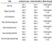
Table 1. Coordinates and areas of defects in Sample-1, 6H Semi-insulation SiC.
Figure 7 shows the mapping of the defects for Sample-3, N-doped 4H SiC. For this sample there is only one defect. This shows that this sample has little intrinsic or doping defects. Figure 8, shows the shape of the defect. As indicated in Table 3, the area of the defect is 0.1045 mm2. The difference between the samples is, more likely a result of the place of the sample in the ingot, although the type of the crystal, 6H vs. 4H, could be also a factor.
3. Conclusions
To the best of my knowledge, this is one of the few studies of defects in SiC substrates using ASM, if not the only one. The study suggests that defects can take any shape and cover an area greater that 0.1 mm2 or a circular area of more than 300 μm diameter. Such defects render the wafer unusable for device or integrated circuit manufacturing, without some sort of repair.
This study can open the door for developing new processes and instruments. First, the study shows that ASM technique is a cost effective technique to evaluate
Table 2. Coordinates and areas of defects in Sample-2, N-doped 6H SiC.
Table 3. Coordinates and areas of defects in Sample-3, N-doped 4H SiC.
the quality of the growth process by characterizing the defect density along the ingot. The study highlights the need for new ASM microscopes, with laser repairing capability. The new instruments would be able to perform investigation of defect repairing process and thermal stress impact on the repaired substrates.
Using both B and C scan microscopy, laser energy and wavelength, that ensure the best recrystallization results, can be determined. C scan determines the

Figure 7. Mapping of defects of Sampe-3, N-doped 4H SiC.
![]()
Figure 8. Magnified images of the defects in Samp1e-3. Images are arranged according to the defect area.
location and the area, and B scan determines the defects Z-locations and thicknesses. With this information, the wave length capable of penetration the material to that depth can be determined, and the energy needed to repair the specific defect size can be estimated. In fact, these proposed methods and instruments can be adopted for other substrates and materials.
Conflicts of Interest
The author declares no conflicts of interest regarding the publication of this paper.
Cite this paper
Abdel-Motaleb, I.M. (2020) Investigation of Inhomogeneity in Single Crystal SiC Wafers Using C-Scan Acoustic Scanning Microscopy. Crystal Structure Theory and Applications, 9, 1-11. https://doi.org/10.4236/csta.2020.91001
References
- 1. Niina, T., Ohta, K., Nakata, T., Matsushita, Y., Uetani, T. and Fujikawa, Y. (1993) Light Emitting Diode Device and Method for Producing Same. US Patent No. 5187547.
- 2. Edmond, J.A. and Suvorov, A.V. (1997) Method of Forming Green Light Emitting Diode in Silicon Carbide. US Patent No. 5604135.
- 3. Chiu, C.-C., Chen, C.-L. and Shih, K.-K. (2003) High Efficiency White Light Emitting Diode. US Patent No. 6614172B2.
- 4. Zhang, Q., Callanan, R., Das, M.K., Ryu, S.-H., Agarwal, A.K. and Palmour, J.W. (2010) SiC Power Devices for Microgrids. IEEE Transaction on Power Electronics, 25, 2829-2896. https://doi.org/10.1109/TPEL.2010.2079956
- 5. Ostling, M., Ghandi, R. and Zetterling, C.-M. (2011) SiC Power Devices-Present Status, Applications and Future Perspective. Proceedings IEEE 23rd International Symposium on Power Semiconductor Devices and ICs, San Diego, CA, 23-26 May 2011. https://doi.org/10.1109/ISPSD.2011.5890778
- 6. Thakkallapally, R., Veesam, V., Abdel-Motaleb, I. and Shen, Z. (2014) One-Directional 3D-SiC MESFET for High Power Applications. Proceedings of the IEEE National Aerospace and Electronic Conference, Dayton, OH, 24-27 June 2014. https://doi.org/10.1109/NAECON.2014.7045766
- 7. Veesam, V., Thakkallapally, R., Abdel-Motaleb, I. and Shen, Z. (2015) Evaluation of Electric Field and Temperature of 3D SiC/Si Normally-off MOSFET for High Power High Speed Applications. Proceedings of the IEEE Electro-Information Technology IEEE-EIT, Naperville, IL, 21-23 May 2015. https://doi.org/10.1109/NAECON.2014.7045767
- 8. Thakkallapally, R., Veesam, V., Abdel-Motaleb, I. and Shen, Z. (2015) Electrical and Thermal Analysis of Vertical Unidirectional 3C-SiC MESFETs on Silicon Substrate. Proceedings of the IEEE Electro-Information Technology IEEE-EIT, Naperville, IL, 21-23 May 2015. https://doi.org/10.1109/EIT.2015.7293416
- 9. Henry, H.G., Augustine, G., DeSalvo, G.C., Brooks, R.C., Barron, R.R., Oliver, J.D., Morse, A.W., Veasel, B. W., Esker, P.M. and Clarke, R.C. (2004) S-Band Operation of SiC Power MESFET with 20 W (4.4 W/mm) Output Power and 60% PAE. IEEE Transaction on Electron Devices, 51, 839-845. https://doi.org/10.1109/TED.2004.828279
- 10. Asmi, S. and Abdel-Motaleb, I.M. (2006) Effect of Traps and Self Heating on the Microwave Performance of SiC MESFETs. The 8th International Conference on Solid State and Integrated Circuit Technology, Shanghai, China, 23-26 October 2006. https://doi.org/10.1109/ICSICT.2006.306553
- 11. Ouaida, R., Berthou, M., León, J., Perpinà, X., Oge, S., Brosselard, P. and Joubert, C. (2014) Gate Oxide Degradation of SiC MOSFET in Switching Conditions. IEEE Electron Devices Letters, 35, 1284-1286. https://doi.org/10.1109/LED.2014.2361674
- 12. Leone, S., Beyer, F.C., Pedersen, H., Andersson, S., Kordina, O., Henry, A. and Janzén, E. (2011) Chlorinated Precursor Study in Low Temperature Chemical Vapor Deposition of 4H-SiC. Thin Solid Film, 519, 3074-3080. https://doi.org/10.1016/j.tsf.2010.12.119
- 13. Chien, F.R., Ning, X.J., Stemmer, S. and Pirouz, P. (1996) Growth Defects in GaN Films on 6H-SiC Substrates. Applied Physics Letters, 68, 2678. https://doi.org/10.1063/1.116279
- 14. Kong, H.S., Glass, J.T. and Davis, R.F. (1989) Growth Rate, Surface Morphology, and Defect Microstructures of β-SiC Films Chemically Vapor Deposited on 6H-SiC Substrates. Journal of Material Research, 4, 204-214. https://doi.org/10.1557/JMR.1989.0204
- 15. Kimoto, T., Miyamoto, N. and Matsunami, H. (1999) Performance Limiting Surface Defectsin SiC Epitaxial p-n Junction Diodes. IEEE Transactions on Electron Devices, 46, 871-477. https://doi.org/10.1109/16.748864
- 16. Duncan, M.D. and Bashkansky, M. (1998) Subsurface Defect Detection in Materials Using Optical Coherence Tomography. Optical Express, 2, 540-545. https://doi.org/10.1364/OE.2.000540
- 17. Nakashima, S. and Harima, H. (2004) Characterization of Defects in SiC Crystals by Raman Scattering. In: Choyke W.J., Matsunami, H. and Pensl, G., Eds., Silicon Carbide. Advanced Texts in Physics, Springer, Berlin, Heidelberg. https://doi.org/10.1007/978-3-642-18870-1_24
- 18. Weyher, J.L. (2006) Characterization of Wide-Band-Gap Semiconductors (GaN, SiC) by Defect-Selective Etching and Complementary Methods. Superlattices and Microstructures, 40, 279-288. https://doi.org/10.1016/j.spmi.2006.06.011
- 19. Dudley, M., Wang, S.P., Huang, W., Carter Jr., C.H., Tsvetkov, V.F. and Fazi, C. (1995) White-Beam Synchrotron Topographic Studies of Defects in 6H-SiC Single Crystals. Journal of Physics D: Applied Physics, 28, A63-A67. https://doi.org/10.1088/0022-3727/28/4A/012
- 20. Dudley, M., Huang, X. and Vetter, W.M. (2004) Synchrotron White Beam X-Ray Topography and High Resolution X-Ray Diffraction Studies of Defects in SiC Substrates, Epilayers and Device Structures. In: Choyke, W.J., Matsunami, H. and Pensl, G., Eds., Silicon Carbide. Advanced Texts in Physics, Springer, Berlin, Heidelberg. https://doi.org/10.1007/978-3-642-18870-1_26
- 21. Dendo, S., Abdel-Motaleb, I., Lowe, K. and Young, L. (1985) Deep Levels in Semi-Insulating LEC GaAs before and after Silicon Implantation. Journal of the Electrochemical Society, 132, 2673. https://doi.org/10.1149/1.2113646
- 22. Hemmingsson, C., Son, N.T., Kordina, O., Bergman, J.P. and Janzén, E. (1997) Deep Level Defects in Electron-Irradiated 4H SiC Epitaxial Layers. Journal of Applied Physics, 81, 6155. https://doi.org/10.1063/1.364397
- 23. Dunn, F. (1959) Ultrasonic Absorption Microscope. The Journal of the Acoustical Society of America, 31, 632. https://doi.org/10.1121/1.1907767
- 24. Kessler, L.W. and Yuhas, D.E. (1979) Acoustic Microscopy. Proceedings of the IEEE, 67, 526-536. https://doi.org/10.1109/PROC.1979.11281
- 25. Semmens, J.E. and Kessler, L.W. (1989) Nondestructive Evaluation of TAB Bonding by Means of Acoustic Microscopy: Overview of Progress Using C-Mode Scanning Acoustic Microscopy. 9th IEEE/CHMT, International Conference on Manufacturing Technology, 12-17 February 1989.
- 26. Briggs, G. and Kolosove, O. (2010) Acoustic Microscopy. 2nd Edition, Oxford University Press, Oxford.
- 27. https://www.ksisam.com/acousticmicroscopy-en/home-acoustic-microscopy.php