Journal of Surface Engineered Materials and Advanced Technology
Vol.09 No.02(2019), Article ID:91941,17 pages
10.4236/jsemat.2019.92002
Characterization of Microstructure Coatings Used in Industry
Maria Richert1*, Ilona Nejman2, Paulina Zawadzka2
1Management Faculty, AGH University of Science and Technology, Cracow, Poland
2Non-Ferrous Metals Faculty, AGH University of Science and Technology, Cracow, Poland

Copyright © 2019 by author(s) and Scientific Research Publishing Inc.
This work is licensed under the Creative Commons Attribution International License (CC BY 4.0).
http://creativecommons.org/licenses/by/4.0/


Received: February 18, 2019; Accepted: April 20, 2019; Published: April 23, 2019
ABSTRACT
The paper describes the research of coatings on the AK9 aluminum alloy substrate and hybrid coatings deposited on graphite substrate. Coatings on the AK9 alloy were deposited by thermal spraying and PVD method (physical vapour deposition). Hybrid coatings consisting of a tungsten interlayer and an external layer of Zr + DLC (diamond-like carbon) and CVD were deposited on the graphite surface. Plasma methods―PVD and CVD―were used. The structure and composition of coatings were analyzed.
Keywords:
Coatings, Thermal Spraying, PVD

1. Introduction
Surface protection is now widely used in almost every area of the economy. It is applied for corrosion protection, abrasive wear protection, high temperatures, antimicrobial protection or the deposited coatings that can be considered a decorative element.
There are many methods of coating surfaces with layers or coatings. Electrolytic coating and anode oxidation are among the older methods, which have been used for many years and are also intensively used nowadays [1] . One of the latest methods is thermal spraying [2] [3] as well as physical and chemical deposition from the gaseous phase [4] [5] [6] . The development of new methods of producing layers and coatings resulted from the avalanche of innovative solutions enabling the creation of new equipment for the production of coatings. The continuous development of knowledge and the possibility of introducing new types of input materials (e.g. nano-powders) have also contributed to the spectacular development of surface engineering [7] [8] . Undoubtedly, the wide range of applications of coatings and the demand of the industry have been the driving force behind many solutions and the constant striving for the improvement of the coating methods. Numerous examples of the application of surface coatings in industrial plants show the rapid transition of solutions from the laboratory phase to the phase of commonly used commercial industrial applications. A spectacular example is coating a wide range of tools with anti-friction coatings. A typical coating used in such cases is the coating of TiN or TiCrN [9] [10] .
The type of coating used results from its future application and from the conditions of the method it has been deposited with.
The method of deposition of a coating or a layer or a combination of coatings, as in the case of hybrid coatings, defines the thickness, hardness, porosity and other characteristics of the formed coating, which is selected from the point of view of the future operation of the tool, machine part or piece of equipment subject to surface treatment.
Since each of the existing coating methods, despite using the same input material, e.g. TiN, will produce a coating with the same chemical composition but with different physico-chemical and geometric characteristics, this results in directing the application of individual coating methods towards specific applications. The TiN coating produced by thermal spraying will have a thickness of several dozen to several hundred micrometers, high porosity and adhesive connection with the substrate [11] [12] . The same coating deposited by physical vapor deposition from vapor phase (PVD) will be 2 - 9 mm thick, compact and will have a chemical connection with the substrate [13] . However, it is to be expected that some of the desired features will not be achieved with single coatings. Therefore, hybrid methods have emerged, which enable creating a “package of layers” in the form of successively superimposed coatings with different properties [14] [15] [16] . Thermal barriers used in aviation for rotor blades of aircraft turbines [17] [18] [19] [20] are one of such examples.
The variety of applications results in a constant search for new coating solutions. With the need to protect the surface, an economic aspect should also be taken into account. The need to reduce expenditure leads to the abandonment of certain solutions despite the visible benefits. Cheaper solutions are often chosen and surface protection is achieved through paint coatings. The field of painting coatings is currently a highly developed branch of industry and is used in almost every aspect of economy and everyday life [21] .
The paper presents examples of construction of various types of coatings produced by thermal spraying, PVD and CVD methods, their properties were compared and characteristic features were presented.
2. Materials and Methods
Coatings tested in the paper were produced by the following methods:
1) The coatings on the AK9 substrate produced by thermal spraying methods:
a) HVOF (High Velocity Oxy Fuel) method was used to form Cr3C2-NiCr 75 - 25 coating.
b) Plasma spraying method was used to form Cr3C2-NiCr 75 - 25 coating.
2) The coatings on the AK9 substrate produced by thermal spraying methods:
a) EB PVD method was used to deposit Cr3C2 coating.
b) ARC PVD method was used to deposit Cr3C2 coating.
3) Hybrid coatings were deposited on graphite substrate by PVD and CVD methods:
a) A hybrid coating consisting of a tungsten layer by EB PVD method and a DLC (diamond-like) layer by PACVD method were deposited.
b) A hybrid coating consisting of a tungsten layer by EB PVD method and subsequently Zr + DLC layer by Arc CVD method were deposited.
Samples for testing, deposited by thermal spraying, were made in industrial conditions of Plasma System S.A. from Siemianowice Śląskie.
The samples obtained by two methods of thermal spraying were tested:
・ High Velocity Oxygen Fuel spraying (HVOF).
・ Plasma spraying (PS).
The HP/JP 5000 Gun Kit was used for HVOF coatings and the MIM 40 device for plasma spraying. Parameters of coating processes using these methods are presented in Table 1 and Table 2. The coatings were deposited on the AK9 alloy substrate.
Coatings by PVD methods were made in industrial conditions of the Institute for Sustainable Technologies in Radom.
The coatings were deposited by two different methods:
・ Electron-beam physical vapor deposition (EB PVD).
・ Electric arc physical vapor deposition (Arc PVD).
The coatings were deposited using the SPECJAL device, which was built in the Department of Surface Engineering of ITeE-PIB (Institute for Sustainable Technologies) in Radom. The device is equipped with an arc current source (Bułat
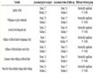
Table 1. Parameters of high velocity oxygen fuel spraying (HVOF).
Table 2. Parameters of plasma thermal spraying.
type) with a cathode with a diameter of Æ80 mm and an electron gun with a power of 60 kW. Inside there is a matrix multi-crucible which contains nine crucibles with a diameter of Æ40 mm in an arrangement of 3 ´ 3. The device is equipped with a three-stage pumping system consisting of a mechanical pump, a Roots pump and a diffusion pump, ensuring stable process conditions. The device is also equipped with a system to control the temperature of the substrate and the pressure of the process atmosphere [21] .
The Cr3C2 carbide coating was deposited on the AK9 alloy substrate using the Arc PVD method using to the conditions shown in Table 3.
For the deposition of Cr3C2 carbide coating by the Arc PVD method, the device is equipped with a 99.9% purity chrome cathode made by the German company GfE.
Prior to coating, the charges were ground and polished in order to obtain a roughness of Ra = 0.01 µm. Next, the samples were washed in a three-chamber ultrasonic cleaner UMO-50-1000 in pure trichloroethylene. The substrate was etched and ionized under the conditions presented in Table 4. C2H5 reactive gas with a flow rate of 50 ÷ 150 ml/min was used in the process.
In the case of the EB PVD method, the charge consisted of chromium, which was placed in a cooled crucible. Due to the very high energy that accumulates in the crucible area (5 - 7 kW) it is not possible to directly evaporate the powders. The material was subjected to sintering into pastilles with a diameter of f = 30 mm and a thickness of g = 5 mm. Pulse Plasma Sintering (PPS) was used for this purpose. Then, the charge material was subjected to the process of electron beam physical vapor deposition in the presence of C2H5 reactive gas with flow between 50 ÷ 150 ml/min. The parameters of this process are shown in Table 5 and Table 6.
Hybrid W/DLC and W/Zr+ DLC coatings were produced on isostatic pressed graphite specimens, the parameters of which are shown in Table 7. This material is used for the production of elements resistant to high temperatures in the
Table 3. Parameters of Cr3C2 coating deposition by Arc PVD.
Table 4. Parameters of etching and heating of the substrate within Arc PVD.
Table 5. Parameters of EB PVD coating processes.
metallurgical industry, e.g. crucibles, crystallizers, die casting moulds, continuous casting sets.
Multilayer coatings W/Zr+DLC were deposited using Arc and electron beam physical vapour deposition technique (Arc-EBPVD), carried out by an original technological process implemented in hybrid multisource device produced by the Institute for Sustainable Technologies The samples were installed in a stationary location opposite the plasma source. Detailed technological parameters of the processes are given in Table 8 and Table 9. The first stage was the application of tungsten layer by EB-PVD method (Table 8). Then, using the Arc PVD method, the substrate was etched with Zr+ ions, and successively the Zr coating was deposited, the substrate was cooled down and then the Zr + DLC coating was deposited. The Zr-DLC coating was generated using a plasma filter, which was an electrostatic separator. A detailed design of the process is discussed in the publication [22] .
Hybrid W/DLC coating was produced using EB-PVD method for tungsten layer formation (Table 8) and PACVD method for external CVD layer formation (Table 10). The IONIT-COMPACT PACVD device, located in the Aviation Industry Research Laboratory at Rzeszów University of Technology, was used. The process included the following stages:
・ heating the reactor chamber to a preset process temperature,
・ nucleation of the diamond coating―hydrogen plasma,
Table 6. Parameters of etching and heating of the substrate within EB PVD.
Table 7. Parameters of graphite substrate.
Table 8. Technological parameters of stage I of W interlayer deposition by EB-PVD method on both samples.
Table 9. Technological parameters of stage II of the deposition process for Zr doped sample (process with the use of an electrostatic separator).
Table 10. Parameters of DLC coating deposition by PA CVD on tungsten coated graphite samples.
・ actual process―plasma mixture H2 + CH4,
・ cooling the reactor.
Hybrid coatings were studied using Thermo Scientific’s Raman DXR Spectrometer to identify the DLC layer. A laser with the wavelength of 532 nm and the power of 10 nW was used. The analysis was carried out in the range of 38 - 3583 cm−1. The results obtained were compared with Raman spectra for diamond and graphite.
The microstructure of coatings was examined by optical microscope Olympus GX51 and Hitachii SU-70 scanning electron microscope (SEM). Thin foils were examined under JEOL 2010 ARB transmission electron microscope (TEM). The samples for optical (OM) and SEM observations were mechanically polished applying Struers equipment and technique. They were ground, then polished with diamond pastes and OPS suspension. Thin foils for TEM investigations were prepared by FIB technique.
3. Results
Figures 1-5 present the results of tests of the structure and chemical
 (A)
(A)
 (B)
(B)
 (C)
(C)
 (D)
(D)
 (E)
(E)
 (F)
(F)
Figure 1. Structure of Cr3C2-NiCr 75 - 25, deposited by HVOF method on the AK9 substrate. (A) Cross-section through coatings, optical microscopy; (B) Chemical composition of the coating, X-ray spectrum; (C) Coating microstructure, optical microscopy; (D) Structure of the coating observed from the top by scanning microscopy; (E) Microstructure observed with a transmission electron microscope, visible nanometric size carbides; (F) Chemical composition determined by EDX method.
 (A)
(A)
 (B)
(B)
 (C)
(C)
 (D)
(D)
 (E)
(E)
 (F)
(F)
Figure 2. Structure of Cr3C2-NiCr 75 - 25 coating, produced by PS on the AK9 substrate. (A) Cross-section through the coating, optical microscopy; (B) X-ray spectrum of chemical composition of the coating; (C) Structure of elongated grains in the coating, optical microscopy; (D) Structure of the coating observed from the top by scanning microscopy; (E) Nanometric microstructure of the coating observed with a transmission electron microscope; (F) Chemical composition determined by EDX method.
 (A)
(A)
 (B)
(B)
 (C)
(C)
 (D)
(D)
 (E)
(E)
 (F)
(F)
Figure 3. Structure of the Cr3C2 coating deposited by EB PVD on the AK9 substrate. (A) Cross-section through the coating, optical microscopy; (B) X-ray spectrum of chemical composition of the coating; (C) Structure of the coating observed from the top by scanning microscopy; (D) Structure of the coating observed from the top by scanning microscopy; (E) Nanometric microstructure of the coating observed with a transmission electron microscope; (F) Chemical composition determined by EDX method.
 (A)
(A)
 (B)
(B)
 (C)
(C)
 (D)
(D)
 (E)
(E)
 (F)
(F)
Figure 4. Structure of the Cr3C2 coating deposited by EB PVD on the AK9 substrate. (A) Cross-section through the coating, optical microscopy; (B) Structure of the coating observed from the top by scanning microscopy; (C) Structure of the coating observed from the top by scanning microscopy; (D) Structure of the coating observed from the top by scanning microscopy; (E) Nanometric microstructure of the coating observed with a transmission electron microscope; (F) Chemical composition determined by EDX method.
composition of coatings made with different methods.
Figure 1 shows the Cr3C2-NiCr 75 - 25 coating, which was produced by HVOF method on the AK9 substrate. The thickness of the coating was estimated to be about 350 µm. The coating contains numerous Cr3C2 carbides evenly distributed in the deposited layer (Figure 1(C)). The presence of carbides of nanometric sizes was confirmed by the examination of thin foils with a transmission electron microscope (Figure 1(E)). The observation of the surface of the coating, from the front, using a scanning microscope, revealed a compact fine-grained structure (Figure 1(D)).
The structure of the Cr3C2-NiCr 75 - 25 coating deposited by plasma spraying (PS) is shown in Figure 2. The thickness of the coating was estimated to be about 200 µm. On the cross-section, parallel to the substrate, grains containing numerous Cr3C2 carbide inside are clearly visible, parallel to the substrate (Figure 2(C)). The view from the top showed the surface with numerous pores (Figure 2(D)). Analysis using a transmission electron microscope showed that the internal microstructure consists of nanometric grains.
Figure 3 and Figure 4 show the structure of coatings deposited by PVD method. Figure 3 shows the Cr3C2 coating deposited by EB PVD method, while Figure 4 shows the coating deposited by ARC PVD method. Coatings are significantly thinner than those obtained by thermal spraying. In particular, the coating deposited using the ARC PVD method (d ~ 1.4 µm) is very thin. The thickness of the coating applied by EB PVD method was estimated to be several micrometers.
The PVD coating has a columnar structure typical for physical vapour deposition coatings. Heterogeneity of the structure is observed in the form of cracks and losses of the material in the deposited coatings and funnel-shaped thickening resulting from disturbances in growth through the droplet phase, occurring in the process of arc evaporation (Figure 3(A)).
The structure of hybrid coatings is shown in Figure 5 and Figure 6.
Figure 5 shows the coating consisting of a tungsten layer deposited by EB PVD method and then the DLC layer deposited by PACVD method. The tungsten layer is 15 µm thick. The existence of the DLC layer was confirmed by Raman spectroscopy (Figure 5(B)). The structure of this system is characterized by the presence of DLC layer of variable thickness in the range of about 20 - 100 nm (Figure 5(C)). It seems that extending the time of DLC deposition could even out the thickness of the layer due to the island nucleation of the DLC phase reported in the literature [23] . Blurred peaks indicate that the structure of the DLC layer is formless.
Figure 5(A) shows a fragment of tungsten layer structure disturbance by droplet phase during layer deposition in PVD device. Such disturbances reduce the smoothness of the top surface as they are reflected in the successive layers.
Figure 6 shows the hybrid coating W/Zr + DLC. The measurements showed that the thickness of the tungsten layer is about 16 µm and the Zr layer about 1.4 µm. The presence of DLC layer was confirmed by Raman study (Figure 6(B)). The Raman spectrum of the Zr + DLC coating (Figure 6/71) is characterized by an extended peak from 1000 to 1700 cm−1, which is characteristic for DLC coatings. The spectrum does not have a characteristic graphite peak at 2700 cm−1. Blurred peaks blur indicate that the structure of the layer is formless.
 (A)
(A) (B)
(B) (C)
(C)
Figure 5. Structure of W/DLC hybrid coating with Raman test results. (A) Microstructure of W/DLC hybrid coating deposited on graphite substrate, SEM. The presence of DLC coating was confirmed―Raman spectrum; (B) Results of Raman analysis of W/DLC coating (comparison of W/Zr + DLC coating spectra with diamond and graphite spectra); (C) Microstructure of individual areas of the W/DLC hybrid coating (TEM), (a) bright field of view, (b) dark field of view, transmission electron microscopy.
The structure of the W/Zr + DLC layer system observed with the transmission electron microscope is shown in Figure 6(C). The study revealed the presence of the Zr layer between the tungsten layer and the Zr + DLC layer. It can be noticed that the Zr layer is about 400 nm thick and the Zr + DLC layer is about 100 nm thick. It is probable that the thickness of the layer can change locally along the length of the sample.
4. Discussion
Investigations of coatings deposited by different methods of surface engineering reveal significant differences in the structure and geometric dimensions of layers.
 (A)
(A) (B)
(B) (C)
(C)
Figure 6. Structure of W/Zr + DLC hybrid coating with Raman test results. (A) Microstructure of hybrid coating W/Zr + DLC deposited on graphite substrate by PVD method: ((a), (b)) optical microscopy (OM), ((c), (d)) scanning electron microscopy (SEM). The presence of DLC coating (Raman spectrum) is found; (B) Results of Raman analysis of W/Zr + DLC coating (comparison of W/Zr + DLC coating spectra with diamond and graphite spectra); (C) Microstructure of individual areas of hybrid coating W/Zr + DLC. Transmission electron microscopy.
This is due to the mechanisms of deposition of coatings leading to their different structures [24] . In the case of thermal spraying, the coating is formed by sticking particles dissolved in a stream of hot gases onto a surface that has previously been cleaned and has the appropriate roughness.
In the gas stream, the individual particles achieve high speeds: ~160 m/s in flame and arc spraying, ~200 - 250 m/s in plasma spraying (PS) and above 330 m/s in supersonic spraying (HVOF). Upon hitting the surface, the droplets cool down and solidify. During the movement towards the surface, the droplets, due to surface tension, are spherical in shape and, when they hit the surface, they are flattened parallel to the surface and take on the characteristic, strongly elongated shape. At this stage, oxides can form on the surface of the droplets, if the spraying is not carried out in the vacuum chamber. Therefore, unmelted particles and oxides resulting from the interaction of powder with air can be found in the structure of thermally sprayed layers and coatings. Thermally sprayed coatings have high porosity, which decreases when using higher spraying speeds and using nanometric powders as charge material. The example of Cr3C2 + NiCr coatings presented in the paper, which are deposited by HVOF ultrasonic spraying (Figure 1) and PS plasma spraying (Figure 2), illustrates well the effect of spraying speed on the porosity of the coating, which in the case of PS is much higher (Figure 2).
Nowadays, thermally sprayed layers are widely used to protect the surface of components such as industrial fan blades, for example. A part of the study, presented in the paper, including Cr3C2 thermally sprayed coatings, was the subject of the project No. NR15000106/2009, and the results of the project were applied in the rotor regeneration and construction industry [25] .
The mechanism of producing coatings by PVD methods is completely different. This results in a different structure of the coating. The coating grows from the substrate by depositing and attaching successive ions of the coating material. In contrast to thermal spraying, the substrate should be as smooth as possible. A build-up of the coating from the substrate results in a columnar, compact structure, without porosity. The growth of coatings takes place in vacuum, which protects the material from oxidation. The layers obtained by PVD method are much thinner than the layers produced by thermal spraying.
Hybrid technologies have developed very strongly in recent years, which through the synergy effect combine the features of different types of coatings, resulting in the possibility of obtaining interesting coatings and best solutions for a given application. PVD coatings and hybrid coatings are used more and more often nowadays, among others, on various types of tools [21] .
An example of a hybrid coating is the W/DLC and W/Zr + DLC coatings on graphite presented in the article. The production of coatings on graphite is extremely difficult and only the use of intermediate layers allows to create the top layer of DLC [26] . The task, which was solved in the project (Polish project No INNOTECH-K2/IN2/9/181851/NCBR/13) was to form a protective layer on graphite crystallizers, which were destructed by sticking liquid cast metal on the porous graphite. Hybrid layers on the surface of which a thin layer of DLC was deposited and identified were successfully formed. This is the prospect of a possible extension of the service life of graphite crystallizers. The financial aspect of surface protection projects remains to be considered. The cost of inputs must be commensurate with the profits generated by the new solutions, which can be verified by the economic market.
5. Conclusions
1) The performed investigations allow recognizing characteristic features of different kinds of coatings. Despite the same chemical composition, the characteristics of coatings are different, depending on the applied method of coating deposition, which determines their application and utility in industry.
2) It was found that there is a possibility of depositing DLC coatings on graphite substrate with the use of an intermediate coating allowing combining a very thin and hard DLC layer with the substrate.
Acknowledgements
The work was supported by Polish projects No INNOTECH-K2/IN2/9/181851/ NCBR/13 and No NR15 0001 06/2009. Authors express great thanks to Prof. dr hab. inż. Jerzy Smolik from Institute of Operational Technology ITE PIB, dr inż. Marek Poręba from Rzeszów University of Technology and Plasma System enterprise from Siemianowice for their help in the production of coatings.
Conflicts of Interest
The authors declare no conflicts of interest regarding the publication of this paper.
Cite this paper
Richert, M., Nejman, I. and Zawadzka, P. (2019) Characterization of Microstructure Coatings Used in Industry. Journal of Surface Engineered Materials and Advanced Technology, 9, 11-27. https://doi.org/10.4236/jsemat.2019.92002
References
- 1. Runge, J.M. and Pomis, A.J. (2006) Understanding Aluminium Anodic Oxide Film Formation: Improving Engineering Properties through Microstructural Modification. XII Ebrats Brasilian Surface Treatment Meeting and II Latin—American Interfinish, Sao Paulo, 10 May 2006. https://pdfs.semanticscholar.org/a97a/d14982c66edddada9f30b271264b6b4d24e5.pdf
- 2. Bhatnagar, N. (2014) Thermal Sprayed Alumina Nanocoatings for Corrosion Prevention. International Journal of Chemical, Environmental & Biological Sciences, 2, 61-64.
- 3. Richert, M.W., Mikulowski, B., Palka, P., Hotlos, A. and Perek-Nowak, M. (2013) The Effect of Chemical Composition and Thermal Sprayed Method on the Chromium and Tungsten Carbides Coatings Microstructure. Journal of Surface Engineered Materials and Advanced Technology, 3, 1-5. https://doi.org/10.4236/jsemat.2013.31001
- 4. Moarrefzadeh, A. (2012) Faculty Member of Mechanical Engineering Simulation and Modeling of Physical Vapor Deposition (PVD) Process. Transactions on Applied and Theoretical Mechanics, 7, 106.
- 5. Fukui, H. (2016) Evolutional History of Coating Technologies for Cemented Carbide Inserts—Chemical Vapor Deposition and Physical Vapor Deposition. SEI Technical Review, 82, 39-45.
- 6. Komarova, F.F., Konstantinova, S.V., Pogrebnjakb, A.D., Pilkoa, V.V., Kozakc, C. and Opielakd, M. (2014) Formation and Characterization of Nanostructured Composite Coatings Based on the TiN Phase. Acta Physica Polonica A, 125, 1292-1295.
- 7. Paksunchai, C., Denchitcharoen, S., Chaiyakun, S. and Limsuwan, P. (2012) Growth and Characterization of Nanostructured TiCrN Films Prepared by DC Magnetron Cosputtering. Procedia Engineering, 32, 875-881. https://doi.org/10.1016/j.proeng.2012.02.026
- 8. Tucker, R.C. (1994) ASM Handbook, Volume 5A: Thermal Spray Technology. ASM International, 497.
- 9. Smolik, J. (2012) Hybrid Surface Treatment Technology for Increase of Hot Forging Dies. Archives of Metallurgy and Materials, 57, 657-664. https://doi.org/10.2478/v10172-012-0070-z
- 10. Giridhar, P. and Subbiah, R. (2016) Effect of AlTiN PVD Coating Thickness on 316L Austenitic Stainless Steel Wear Resistance. International Journal of Aerospace and Mechanical Engineering, 3, 19.
- 11. Szczucka-Lasota, B. and Wolniak, R. (2017) The High Quality of Hybrid Sprayed Coatings for Power Plant Application. Zeszyty Naukowe Politechniki Slaskiej, 469-480.
- 12. Song, C., Liu, M., Deng, Z., Peng, S., Chun, N., Deng, M. and Liao, H.L. (2018) A Novel Method for In-Situ Synthesized TiN Coatings by Plasma Spray-Physical Vapor Deposition. Materials Letters, 217, 127-130. https://doi.org/10.1016/j.matlet.2018.01.068
- 13. Su, Y.J., Trice, R.W., Faber, K.T., Wang, S.H. and Porter, W.D. (2004) Thermal Conductivity, Phase Stability, and Oxidation Resistance of Y3Al5O12 (YAG)/Y2O3-ZrO2 (YSZ) Thermal-Barrier Coatings. Oxidation of Metals, 61, 253-271. https://doi.org/10.1023/B:OXID.0000025334.02788.d3
- 14. Montemor, M.F. (2014) Functional and Smart Coatings for Corrosion Protection: A Review of Recent Advances. Surface and Coatings Technology, 258, 17-37.
- 15. Kennedy, D., Xue, Y. and Mihaylov, M. (2005) Current and Future Applications of Surface Engineering. The Engineers Journal (Technical), 59, 287-292.
- 16. Rivero, P.J., Urrutia, A., Goicoechea, J., Zamarreno, C.R., Arregui, F.J. and Matías, I.R. (2011) An Antibacterial Coating Based on a Polymer/Sol-Gel Hybrid Matrix Loaded with Silver Nanoparticles. Nanoscale Research Letters, 6, 305. https://doi.org/10.1186/1556-276X-6-305
- 17. Padture, N.P., Gell, M. and Jordan, E.H. (2002) Thermal Barrier Coatings for Gas-Turbine Engine Applications. Science, 296, 280-284. https://doi.org/10.1126/science.1068609
- 18. Wellman, R.G. and Nicholls, J.R. (2007) A Review of the Erosion of Thermal Barrier Coatings. Journal of Physics D: Applied Physics, 40, R293. https://doi.org/10.1088/0022-3727/40/16/R01
- 19. Paint and Coatings Market Research Reports. https://www.marketreseArchhub.com/paints-and-coatings-market-reports.html?page=10
- 20. Smolik, J. (2016) Hybrydowe Technologie Inzynierii Powierzchni. Biblioteka Problemów Eksploatacji, Wyd. Naukowe Instytutu Technologii Eksploatacji PIB, Radom.
- 21. Richert, M., Zawadzka, P., Mazurkiewicz, A., Smolik, J., Leszczyńska-Madej, B., Nejman, I., Palka, P. and Pietrzyk, S. (2016) Deposition of W/a-C:H:Zr and W/a-C:H:W Multilayer Coatings on Substrate Made of Porous Graphite by Arc-Electron Beam Hybrid Method. Surface and Coatings Technology, 300, 19-24.
- 22. Liu, H. and Dandy, D.S. (1995) Studies on Nucleation Process in Diamond CVD: An Overview of Recent Developments. Diamond and Related Materials, 4, 1173-1188. https://doi.org/10.1016/0925-9635(96)00297-2
- 23. Richert, M. and Zawadzka, P. (2014) Utility Coatings on Tools and Machine Parts for the Non-Ferrous Metals Industry. Obróbka Plastyczna Metali, 25, 5-26.
- 24. Richert, M., Ksiazek, M., Leszczyńska-Madej, B., Nejman, I., Grzelka, R. and Palka, P. (2010) The Investigations of Coatings Deposited by Thermal Spraying Methods. Journal of Achievements in Materials and Manufacturing Engineering, 38, 95.
- 25. Wei, Ch., Wang, Y.S. and Tai, F.C. (2009) The Role of Metal Interlayer on Thermal Stress, Film Structure, Wettability and Hydrogen Content for Diamond like Carbon Films on Different Substrate. Diamond and Related Materials, 18, 407-412. https://doi.org/10.1016/j.diamond.2008.11.009
- 26. Ramesham, R. (1999) Voltammetric Studies at the Polycrystalline Diamond Grown over a Graphite Electrode Material. Thin Solid Films, 339, 82-87. https://doi.org/10.1016/S0040-6090(98)01090-6