Enhancement of InGaN-Based Light Emitting Diodes Performance Grown on Cone-Shaped Pattern Sapphire Substrates ()
1. Introduction
InGaN-based light-emitting diodes (LEDs) are useful for a wide range of visible light applications [1] -[4] . They are commonly used in traffic signals, liquid crystal display backlights, microprojectors, car headlights, and full color displays, among other applications. Though high brightness InGaN-based LEDs are commercially available, threading dislocations (TDs) with a density of 108 - 109 cm−2 remain in the LED structures due to the large differences of lattice constant and thermal expansion coefficient between the GaN epilayer and the sapphire substrate. The external quantum efficiency (EQE) of the InGaN-based LED is still not large enough compared with the expected value. EQE is affected by both internal quantum efficiency (IQE) and the light extraction rate. Therefore, how to further reduce the dislocation density is an important issue for fabricating high-performance LEDs. Moreover, the reflective index of nitride films is higher than that of air and sapphire substrate. Most of the light generated in the active layer is absorbed by the electrode at each reflection and gradually disappears, due to total internal reflection (TIR). Although many methods for growing high-quality GaN layers, such as epitaxial lateral overgrowth (ELOG) [5] [6] , pendeo-epitaxy (PE) [7] and lateral overgrowth from trenches (LOFT) [8] have been proposed to reduce the TD densities, all of these techniques inherently suffer from intermediate ex situ processing steps, and typically require multiple MOCVD growths with interruptions, and often introduce doping or induce contamination and result in a much lower production yield [9] .
In recent years, the patterned sapphire substrates (PSS) technique as a maskless and growth interruption-free means has proved to be another feasible approach to reducing the TD density and the percentage of total internal light reflection through its geometrical effect [10] [11] . The different pattern shapes of the PSS were fabricated [12] -[16] by combining conventional photo lithography and dry or wet etching technique, and could be used to effectively scatter or redirect the guided-light inside an LED chip to find escape cones. Besides, different pattern sizes of the PSS have been studied to improve the light extraction of the LEDs [16] -[19] .
In this study, we describe the fabrication, optical and electrical properties of InGaN LEDs on CPSS by using MOCVD. The characteristic improvement of the LED fabricated on CPSS compared with LED on USS is depicted here. In addition, the structural analysis of these LEDs was observed by an atomic force microscope (AFM) and an transmission electron microscopy (TEM).
2. Experiment
Samples used in this study were all grown on c-face (0001) 2 inch sapphire substrates in a vertical MOCVD system. Prior to the MOCVD growth, to prepared CPSS, we used thermal photo resist (PR) reflow and dry etching method. To transfer the pattern to the sapphire substrate, dry etching was carried out by an inductively coupled plasma system (ICP) with a gas mixture of BCl3 and Cl2. The diameter and interval of each cone-shape pattern were 2.5 μm and 0.5 μm respectively, and the height of a cone shape was about 1.6 μm. A scanning electron microscopy (SEM) image of the cone-shaped patterns is shown in Figure 1.

Figure 1. Plan-view SEM images of CPSS. The inset shows single cone image.
After fabrication, blue InGaN/GaN LEDs were grown on CPSS using metal organic chemical vapor deposition (MOCVD). Trimethylgallium (TMGa), trimethylaluminum (TMAl), trimethylindium (TMIn), and ammonia (NH3) were used as precursors. Silane (SiH4) and bis(cyclopentadienyl)magnesium (Cp2Mg) were used as the n-dopant and p-dopant sources. The LED structure consisted of a 30 nm thick GaN nucleation layer, a 3 μm thick undoped GaN layer, a 2 μm thick highly doped n-type GaN layer, six pairs of InGaN (2.5 nm)/GaN (12.5 nm) multiple quantum wells (MQWs), a 20 nm thick p-type AlGaN electron blocking layer, and a 150 nm thick Mg-doped GaN layer. The u-GaN growth temperature was increased to 1120˚C to achieve better coalescence on the patterned sapphire substrate.
For the standard LED process, ICP dry etching technique was used to etch through the p-GaN layer and MQW active region, until the n-GaN layer was exposed. Indium tin oxide (ITO) was deposited onto the p-GaN layer by e-beam evaporator, and then thermally annealed in oxygen ambient for 12 min. The ITO layer was used as the transparent contact layer. The Cr/Pt/Au metals were deposited as the p-and n-electrodes by e-beam evaporator. For comparison, conventional InGaN/GaN MQW blue LED grown on the USS were also prepared with exactly the same growth and process conditions. The crystalline quality of the grown LEDs was investigated by atomic force microscopy (AFM) and TEM. Using a semiconductor laser (405 nm) as the exciting source, the photoluminescence (PL) was used to evaluate the devices’ optical properties. The output powers were measured using the molded LEDs with the integrated sphere detector from top of the devices.
3. Results and Discussion
The surface morphologies of LED wafers grown on CSS and on the CPSS were characterized by atomic force microscope (AFM) as shown in Figure 2(a) and Figure 2(b). No significant difference was observed from these two AFM images. The measured root-mean-square roughness (RMS) is 0.36 nm for LED on CPSS and 0.58 nm for LED on USS. A relative low RMS on CPSS implies that reduced dislocation density and low strain in LED on CPSS can lead to smooth surface.
In order to elucidate the relationship between the optical and structural properties and for a correlation with the lateral growth mode on the cone-shaped patterns, cross-sectional TEM experiment for GaN on CPSS was carried out, as shown in Figure 3. Above the slope region of the cones, many TDs were also generated at the initial growth stage, but most of these TDs did not propagate vertically to the GaN surface but bent as progressing GaN epitaxial growth due to the induced lateral overgrowth mode. As the growth proceeds up to the top of the cone area, the laterally overgrown GaN regions become coalescent and cover the entire cone area, resulting in localized dislocations at the apex of the cone patterns. The presence of bent TDs by 90˚ is evidence of a lateral overgrowth mode playing an important role in the decrease of the TDs.
 (a)
(a)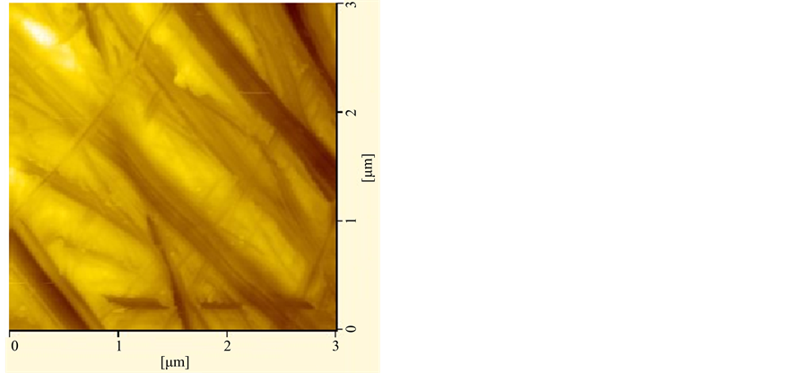 (b)
(b)
Figure 2. (Color online) AFM images of the surfaces of LEDs: (a) On CPSS; (b) On USS.

Figure 3. Cross-section TEM image of GaN epilayer grown on patterned sapphire substrate.
Figure 4 shows the results of PL spectra of the LEDs on CPSS and USS measured at room temperature. A sharp and narrow PL spectrum was observed for LED on CPSS at 457 nm compared to LED on USS. The emission peak intensity was high for LED on CPSS compared to USS. This increase in peak intensity indicates that the crystalline quality was improved significantly and the TD density was reduced for the LED on CPSS. This enhancement was due to the internal reflection on the cones of the substrate. In addition, the full widths at half maximum (FWHM) values for the samples on CPSS and on the USS were 16.02 nm and 22.14 nm respectively. The FWHM value for the LED on the CPSS is smaller than that of the LED on USS, suggesting that the crystalline quality was considerably improved by using the CPSS.
Figure 5(a) displays the current-voltage (I - V) characteristics of PSS LEDs on CPSS and USS with the same chip size as a function of forward driving current. The LEDs on CPSS and USS have low operating voltages, and sharp turn-on voltages near 2.57 and 2.62 V respectively. The forward voltage for the LED on CPSS and USS were 3.10 and 3.22 V at the forward injection current of 20 mA. The forward voltage of LED on CPSS was smaller than that of LED on USS; also the forward I - V curve of LED grown on CPSS didnot show any significant difference with that USS. Almost identical I - V curves infer that the patterning on the LED surface had very little impact on the I - V characteristics.
Figure 5(b) shows the light output power as a function of injection current (L-I) characteristics for the LEDs. The output power of LED on CPSS is larger than that of LED on USS at the case of the same injection current. Under a 20 mA forward injection current, the light output powers of LEDs on CPSS and USS were about 29.14 and 17.28 mW. Therefore, an enhancement in output power is attributed to an increase of the extraction quantum effciency by suppressing total internal reflection at the corrugated interface and partially improving the crystal quality due to the reduction of dislocations. The key to enhancing the output power is to give the photons multiple opportunities to find the escape cone. The patterned substrate can redirect photons that were originally emitted out of the escape come back into the escape cone on the top of device surfaces. This indicates that the probability of photons escaping from the LED on CPSS is increased, resulting in an enhancement light extraction efficiency. After reaching the maximum at 349 mA for LED on CPSS and 289 mA for LED on USS, the output powers decrease as the injection current further increases. The decrease in output power is attributed to the thermal dissipation problem. It is well known that carrier recombination occurring in defects and/or dislocations is non-radiative, and such non-radiative recombination will result in heat generation. Because the dislocation density in LED on CPSS is much smaller, the thermal-dissipation problem will be less severe. As a result, the maximum output power will be larger and also occur at a larger injection current for LED on CPSS.
4. Conclusion
In this study, InGaN-based blue LEDs grown by MOCVD on CPSS and USS were investigated. The AFM image reveals a smooth surface on LED-CPSS. From cross section TEM observation, most TDs above the slope region of the cones were bent by lateral growth, therefore there are fewer or almost no TD above the slope re-

Figure 4. Photoluminescence (PL) measurement at room temperature for LED on CPSS and USS.
 (a)
(a) (b)
(b)
Figure 5. Curves of current-voltage (I-V) (a) and light output power in relation to injection current (L-I) (b) for LEDs on USS and CPSS.
gion of the cones. The PL spectra clearly indicate good optical quality of LED on CPSS due to the reduction in TD density and the improvement in the light emission efficiency. The improvement of the output power is mainly due to the enhancement of the extraction efficiency using the CPSS and partly due to the improvement of the internal quantum efficiency by decreasing the dislocation density. The facets of substrate patterns effectively redirect the light to the top escape-cone of the LED surface.
Foundation Item
Project supported by Natural Science Foundation of Hunan Province (Grant No. 13JJ3121).
NOTES
*Corresponding author.