Mitigating Time Interval Error (TIE) in High-Speed Baseband Digital Transports: Design for Delay Compensation at Baseband Infrastructure of Smart-Phones Using Fractal Dispersive Delay-Lines ()
1. Introduction
In the context of the state-of-the-art smart-phones and other mobile/hand-held devices, the data bit-rates adopted at baseband levels could be significantly high (~500 Mbps); and, such streams of high-speed bits are often transferred between chips and/or various circuit nodes during baseband signal-processing, for example, between an image-sensor and an image sensor processor (ISP). To negotiate such transfers, numerous copper-traces are envisaged at the board-level formed either on a single surface or in multiple board/flex stacks. Normally, such trace-lines are of different lengths so as to accommodate ad hoc interconnections and digital transits between the pins across any two devices placed at distinct locations on the board. Further, several of these lines may run almost parallel to each other with jagged tracks. An example of such a track is illustrated in Figure 1.
As a result of varying physical lengths of the traces, the digital bits transported from one end on any given trace will arrive at the pin of signal destination (terminated on the chips in question) with a specific extent of transmission-line dependent delay. However, this delay could be distinctly variable in each of the traces due to varying path-lengths involved and varying bit-rates of information transmitted. That is, the observed delay is specific to each line-length as defined by the associated line-parameters namely, the inductance and the capacitance per unit length and the digital signature of the information communicated. The resulting data dependent jitter (DDJ) [1] introduces time interval error (TIE) (also known as phase jitter) perceived invariably on the bits. Given the spatial features (length etc.) of the high-speed line (transmission topology) and the associated data transceived, the DDJ and the associated TIE can be viewed as a class of deterministic timing jitter. It is an undesired artifact and may cause flicker in displays (of the camera etc.). It would also affect the performance of the digital processors at large.
Hence, the data pulses received with varying delays traversing different parallel lines may become unusable for applications and digital-processing efforts at the receiving devices due to the associated randomness of delay variations tied to the TIE. Therefore in practice, delay-lines are introduced in each trace to compensate for the transit-delay so that the digital data supported are displaced in time on ad hoc basis and get synchronized at the receiving end as needed minimizing the influence of TIE.
Traditionally, at circuit-board level, physical inductors in solenoidal forms are designed, trimmed and incorporated on transmission-lines so as to offer a desired inductance (especially at RF sections) [2] . However, such a conventional (solenoidal) inductor element on a circuit-board implies a complex component-accommodation task due to the bulky, three-dimensional geometry of the solenoid designed for baseband applications. Therefore, relevant option is not conducive for applications in systems like smart-phones and other handheld devices encountering restricted space. Alternative to bulk solenoidal inductors, advocated in practice for space-constrained circuit-board applications is planar geometry of copper-traces (such as spiral traces) designed to emulate the desired inductance values [3] [4] .
Yet, considering the specific needs of modern smart-phones or similar handheld gizmos vis-à-vis emulating tailor-made extents of delays compatible for high-density traces (at baseband levels), a novel design is proposed in this paper toward synthesizing a new class of planar inductors using fractal geometry. Shown in Figure 2 is the geometry of a conceivable module of distributed delay-line (DDL) based on spiral circular or square-loop geometry conforming to a fractal structure. Shown in Figure 3 is the photograph of the circular-spiral fractal inductance used in the present study.

Figure 1. Example of copper-trace route on a typical printed circuit-board layout.
 (a) (b)
Figure 2. A set of spiral inductors configured as a planar fractal delay-line: (a) with circular-spirals and (b) square-spirals.

Figure 3. Photograph of the distributed delay-line (DDL) on a PCB made based on circular spiral fractal geometry: Test module studied conforming to Figure 2(a).
It is surmised in this study that the fractal planar inductors can be designed to facilitate a desired delay-time in a constrained on-board area. Apart from spiral, other options such as meander line, Hilbert structure, Minkowski curve, Koch’s curve etc. can be adopted in making fractal geometry. Conceived thereof in vogue, are structures to optimize the delay-line performance versus space-filling considerations as warranted in baseband, high-speed operations of smart-phones and/or similar devices. Associated higher order fractal curves enable design options with good space-filling properties. Most of such fractal structures have been conceived in the contexts of antenna designs and related RF units as reported in [3] -[11] . The underlying considerations are however, can be borrowed in conceiving fractal inductance as time-delay lines.
This paper is organized to describe a test study on a proto-type of fractal inductor geometry illustrated in Figure 2(a) and Figure 3, which is commensurate with practical aspects of its implementation as a delay-line in high-speed digital transports at baseband operations at the infrastructure of smart-phones (and/or similar handheld devices). Experimental results obtained from the test module are presented to illustrate the efficacy of the module and realizable delay performance vis-à-vis the digital transports of interest. Thus, the scope of this paper in essence is evolved to provide an overview of general details on digital information transmission/ processing at baseband levels of modern smart-phones and similar gadgets of different technologies; and, indicated the conceived fractal geometry as a plausible delay-line structure for combating the TIE.
2. Digital Data Format Seen at Baseband in Smart-Phones or Similar Devices
The physically transmitted baseband signal represents a “digital-over-digital” transmission of pulse trains. In modern context of 3G through 4G considerations and associated LTE implications, the baseband data handled in the infrastructures of smart-phones (and similar devices) is used at specific versions of processors with chip-designs and system-on-chips (SoCs) that accommodate generous audio, and video digital signal processing. Such processors are required to meet multi-standard integration, reduced power dissipation and facilitate extra key functions for next-generation smart, handheld devices. Relevantly, baseband processors provide efficient operations with cost-effective multimedia application-specific processing for entry-level 3G as well as next-generation/evolving 4G systems. Further, in such complex baseband chip-specific operations, the underlying applications invariably dictate the use of high-speed bit rates.
For example, considering video-processing support for 10/12 Mpixels imaging and 720 p video-playback plus accelerated 2D/3D graphics, operational needs push the processor speeds up to 1GHz or even higher. Concurrently, related transmissions point out the gravity of multiple high-speed transports on the limited-space circuitboard (and/or flexible-board) layouts. Together with the packaging designs of the components and chips on the board, the interconnections that support the said digital transports are crowded and routed haphazardly. Hence, the transmission-lines (traces) envisaged thereof are high in density (per unit area) and of varying lengths. Therefore, the digital transports end up in TIE-related issues that call for effective mitigations.
3. Architectural Layouts of Baseband Infrastructures
Commensurate with the types of digital processors and interconnections mandated at the baseband infrastructure, the circuit-board and/or flex-boards have to be carefully designed in practice and traces should be laid out with minimized lengths and routing to avoid not only the TIE, but also crosstalk effects. Specifically, the items of planar structure needed for TIE mitigation via inductor emulations as delay-lines are described below with relevant basics.
Planar Inductors: An Overview
Variety lies in conceiving delay-line topologies and basically, planar delay-lines are made using meander-lines or spiral-line configurations. Functionally, a delay-line offers a desired extent of time-delay between circuit components. In digital domain such delay requisites have been achieved classically with phase-shifting electronic switches [12] . However, considering component reduction efforts and miniaturization warranted in systems like mobile devices, planar passive delay-lines are more congenial and are often resorted to. Typically, the meander-line that has a serpentine form of a closely-packed transmission-line structure can be designed with high density per square mm of circuit-board space.
However, such serpentine delay structures may introduce spurious dispersions that signal appear along with the signal as if, it is arriving earlier than would be expected, as decided by the total electrical length of the line. This is typical with the disposition of two or more adjacent lines closely spaced; further, such proximal layout would lead to electromagnetic (EM) coupling as well and related crosstalk effects [13] [14] . The adjacent line interaction and related skew on the digital waveform is also decided by the loss-tangent of the circuit-board material implicating the associated mutual capacitive and inductive effects on the signal. In order to avoid such laddering effects [4] , a tangible pursuit is to have some planar geometry laid out in sections over a permissible area. For example, using typical circular and square spiral-lines, a few of such geometries can be interconnected into a fractal forms as illustrated earlier in Figure 2. Hence, proposed in the present study is a novel technique to realize a class of inductors based on a distributed set of spiral inductors framed in fractal geometry. Such a line is studied to emulate delay-line corrections in timing sensitive circuits of the baseband infrastructure in smart hand-held devices.
Traditionally, as mentioned earlier, fractal structures on printed circuit-boards have been advocated in practice toward emulating fractal antennas, fractal capacitors and fractal inductors [3] -[11] . All such efforts aim at downscaling/sizing the passive planar component dimensions for applications on the printed circuit-boards. In contrast with inductors of solenoidal form (of three-dimensional structure requiring large space), the fractal curve geometries are evolved in 2D with a potential solution toward compact inductance realization.
Higher order fractal curves are characterized with good space-filling properties and tend to show better efficiency than standard inductance structures having the same overall dimensions. As such, fractal-based RF structures have emerged successfully in making of capacitors, antennas and related resonating components. Fractals are a class of non-Euclidean geometries with unique attributes. A fractal design conforms to a self-similar geometry that maximizes the length or increases the parameter of a unit in emulating a desired EM characteristic within a given total surface area or volume. Fractal structures, in general, are referred to as multilevel and space-filing curves with the repetition of a motif over two or more scale sizes. With the iteration of the motif thereof, fractal structures are compactly formed. For example, as proposed in the present study, a fractal inductance can be formed as a space-filling curve in the shape of a shrunken fractal helix (Figure 2). And, the resulting structure is studied of its delay-line characteristics compatible for use in the baseband infrastructure of smart-phone etc. Described below are some fundamental considerations in designing simple fractal delay-line structures.
Basically planar components like capacitors and inductors can be fabricated as printed elements with small tolerances using the modern artwork of photolithographic process relevant to printed-circuit boards [2] . Traditional, stand-alone meander and spiral structures conceived are illustrated with descriptive notes in Table 1 with typical design (empirical) parameters concerning various inductor geometries illustrated. Using such basic 2D geometries, their fractal forms can be obtained with necessary analogies and tests. The fractal version of using the stand-alone units, for example, relevant to a circular spiral loop as adopted in the present study is shown in Figure 2(a) and Figure 3. It is essentially a planar single-layer two-port structure. It can be equivalently modeled by a standard π-network to include any associated parasitic and conductive (resistive) properties such as, the board-leakage and series self-resistance of the copper traces. The overall equivalent circuit of inductance emulation with the associated parasitics is shown in Figure 4 with reference to a single spiral.
Figure 5 are typical planar geometries adopted in practice to emulate inductances on PCB that can also be used as compatible delay-lines. Indicated in Table 1 are pertinent details of the geometries in Figure 5. Relevant formulations are mostly empirical but, are very useful in practical designs.
4. Test Inductance/Delay-Line: Description and Measurements
The test inductor for the intended delay-line application is fabricated as a single-layer copper trace structure on the top of a standard printed circuit-board using conventional photolithographic process. As illustrated earlier in Figure 2 and Figure 3, the test unit has eleven circular spirals with overall dimensions and details as given in Table 2.
Measurement studies on the test fractal inductor are performed to estimate the time-delay on a signal at a given frequency that can be achieved by considering two or more spirals at a time. Relevant circuit used for testing is shown in Figure 6 and the corresponding time-delay data measured is presented in Figure 7 as a function of the test frequency. This delay is obtained in terms of the phase-shift observed relevant to the input and

Figure 4. Equivalent circuit representation of a planar inductor conceived with a spiral (L: Inductance, Rs: Inherent series resistance, Rp: Leakage resistance, and Cp: Parasitic capacitance).
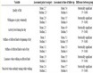
Table 1. Typical planar geometries (of Figure 5) that can be used to emulate inductance and related delay-lines.
Planar geometry
Table 2. Dimensional details of the test fractal inductor (Figure 2 and Figure 3 ).

Figure 7. Measured delay (δ) normalized with respect to the signal period (T), versus signal frequency (f) in MHz, (L1 to L11 etc.: Number of spirals in the fractal geometry cascaded and tested).
output waveforms of the test circuit. Typical scope-plots are shown in Figure 8(a) and Figure 8(b) at two exemplar measurement frequencies of 40 MHz and 80 MHz (relevant to series-connected 5 and 10 spirals in the test fractal geometry respectively).
The time-delay (d) is obtained from the measured phase shift (f) across the series-connected L-structures used in the test. It is presented in normalized values with respect to the signal period (T) in Figure 7 as a function of frequency. As indicated, the set of graphs furnished corresponds to measured values of the normalized delay offered by two or more spirals taken in succession. Hence, the top-most curve conforms to the case with the largest inductance due to all the eleven spirals cascaded; and, the bottom-most curve corresponds to the last-two
 (a)
(a)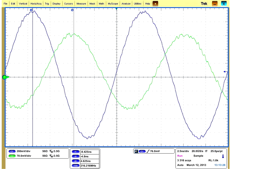 (b)
(b)
Figure 8. (a) Waveforms measured at the input and output at 40 MHz for 5 spirals (L1 through L5 serially connected in the fractal structure); (b) Waveforms measured at the input and output at 80 MHz for 5 spirals (L1 through L10 serially connected in the fractal structure).
spirals (L10 and L11) of the fractal geometry. It can be consistently observed in Figure 7 that the variation of time-delay (or implicitly, the phase-shift) increases monotonically with signal frequency. However, the test curves also show peaks and valleys at certain frequencies implying possible resonances due to the associated parasitic capacitances of the system and related Q factors.
Based on the novel concept structure and achievable delay demonstrated in the prototype model studied, more work can be exercised as regard to other fractal structures such as square-loop version, Koch fractal geometry, Hilbert fractal curve etc. Fabrication issues like ground-plane/ground counterpoise effects and circuit-board layer considerations need more careful studies. The proposed strategy may however, pose fabrication and/or manufacture difficulties at present. But, the technology details as in [6] [15] -[18] show lead pursuits on relevant realizations for practical considerations in view of evolving miniaturized scaled-down designs.