World Journal of Nano Science and Engineering
Vol.06 No.04(2016), Article ID:73159,12 pages
10.4236/wjnse.2016.64016
Study of Timing Characteristics of NOT Gate Transistor Level Circuit Implemented Using Nano-MOSFET by Analyzing Sub-Band Potential Energy Profile and Current-Voltage Characteristic of Quasi-Ballistic Transport
Chek Yee Ooi1, Soo King Lim2
1Faculty of Information and Communication Technology, Universiti Tunku Abdul Rahman, Jalan Universiti, Bandar Barat, Kampar, Perak, Malaysia
2Lee Kong Chian Faculty of Engineering and Science, Universiti Tunku Abdul Rahman, Jalan Sungai Long, Bandar Sungai Long, Cheras, Kajang, Selangor, Malaysia
![]()
Copyright © 2016 by authors and Scientific Research Publishing Inc.
This work is licensed under the Creative Commons Attribution International License (CC BY 4.0).
http://creativecommons.org/licenses/by/4.0/


Received: December 8, 2016; Accepted: December 26, 2016; Published: December 29, 2016
ABSTRACT
This paper presents the quasi-ballistic electron transport of a symmetric double-gate (DG) nano-MOSFET with 10 nm gate length and implementation of logical NOT transistor circuit using this nano-MOSFET. Theoretical calculation and simulation using NanoMOS have been done to obtain parameters such as ballistic efficiency, backscattering mean free path, backscattering coefficient, critical length, thermal velocity, capacitances, resistance and drain current. NanoMOS is an on-line device simulator. Theoretical and simulated drain current per micro of width is closely matched. Transistor loaded NOT gate is simulated using WinSpice. Theoretical and simulated value of rise time, fall time, propagation delay and maximum signal frequency of logical NOT transistor level circuit is closely matched. Quasi-ballistic transport has been investigated in this paper since modern MOSFET devices operate between the drift-diffusion and ballistic regimes. This paper aims to enable modern semiconductor device engineers to become familiar with both approaches.
Keywords:
Theoretical, Simulation, Nano-MOSFET, Transistor Level, Quasi-Ballistic

1. Introduction
In traditional semiconductor devices, carriers are frequently scattered from phonons, ionized impurities and surface roughness. In the traditional devices, the backscattering mean free path λ is much shorter than the device channel. So, drift-diffusion approach is used to describe the carrier transport. However, as devices downscale to nanometer regime, backscattering mean free path become comparable to transistor dimensions. When the backscattering mean free path becomes much larger than the transistor channel length, scattering can be totally ignored. In this situation, a nano-MOSFET behaves like a vacuum tube. In practical devices, scatterings are unavoidable in semiconductor devices. Therefore, modern devices operate in quasi-ballistic mode which is between drift-diffusion and ballistic regimes. Put in other words, drift-diffusion theory is no longer strictly valid as well as ballistic treatment. Hence, modern device engineer must familiar with both approaches. Then, the nano-MOSFET studied in this paper is applied in implementing logical NOT transistor level circuit [1] [2] [3] [4] .
2. Theory and Methodology
Silicon (Si) MOSFETs currently operate between the ballistic and diffusive limits; the scattering model provides a conceptual model for transport in this quasi-ballistic regime. In this scattering model, the most important scatterings occur in the low-field region near the beginning of the channel at source side. Carrier scattering in the channel reduces the current and can be described by ballistic efficiency. Scattering model predicts that the drain current is close to the ballistic limit under high drain bias than under low drain bias, and the on-state current in strong inversion is limited by a small portion of the channel near the source, that is the top region of sub-band potential barrier.
The double-gate (DG) nano-MOSFET structure used in NanoMOS simulation is shown in Figure 1 with simulation structural parameters listed in Table 1.
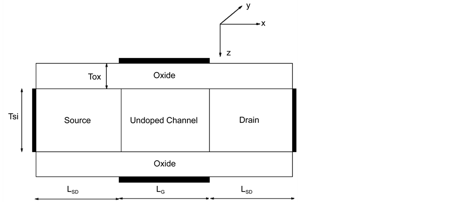
Figure 1. Structural DG Nano-MOSFET used in nanoMOS simulation tool.
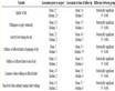
Table 1. Double gate nano-MOSFET device simulation parameter.
The on-state current of the nano-MOSFET is controlled by a short low-field region close to the source end of the channel. The length l of this area is called critical length which is defined as the distance from the peak of the potential barrier to the point
where the potential reduces by .
.  is a numerical factor ≥1. This factor has a
value of 1 for non-degenerate case and slightly greater than 1 for degenerate case. In this paper, take .
.  is the backscattering mean free path. Then, the backscattering coefficient r is given by
 (1)
(1)
The ballistic efficiency B is given by
 (2)
(2)
 (3)
(3)
where electron mobility at ballistic transport in Silicon is ![]() cm2/Vs. The thermal velocity is given by
cm2/Vs. The thermal velocity is given by
![]() (4)
(4)
where ![]() and T = 300 K. The critical length is given by
and T = 300 K. The critical length is given by
![]() (5)
(5)
Since lower bound for ![]() is used at diffusive transport and upper bound for
is used at diffusive transport and upper bound for ![]() is used at ballistic transport,
is used at ballistic transport, ![]() is used at quasi-ballistic transport.
is used at quasi-ballistic transport.
In studying the theoretical part of this paper, the following Fermi-Dirac integrals are used:
![]() (6)
(6)
![]() (7)
(7)
![]() (8)
(8)
where
 (9)
(9)
 is the average energy between source and drain in sub-band energy profile whereas
  is the energy level at the center of the device. Next, the following expression is used to analyze the drain current per micron of width:
 (10)
(10)
After considering the ballistic efficiency B,
 (11)
(11)
 (12)
(12)
is the gate oxide capacitance per unit area
 (13)
(13)
 (14)
(14)
 is the average energy between source and drain in sub-band energy profile whereas
  is the energy level at the region around top of the potential barrier. This region limits on-state current because scatterings mostly occur in this region. In analyzing Equation (10) and Equation (11), the following Fermi-Dirac integrals are used:
 (15)
(15)
 (16)
(16)
The on-line current-voltage (I-V) simulation result of NanoMOS is compared with theoretical calculation using Equation (11).
In order to calculate resistance RLoad of nano-MOSFET at quasi-ballistic limit, uses
 (17)
(17)
Since digital logic gates operate at linear portion of I-V curve. This RLoad is used in analyzing rise time of transistor loaded NOT gate circuit. On the other hand, the following expression is used to obtain on-state channel resistance Rchannel at on-state which is used in fall time analysis.
 (18)
(18)
 = electron mobility at ballistic = 1200 cm2/Vs.
 = Oxide capacitance per unit area.
Transistor loaded NOT gate as shown in Figure 2 is simulated using WinSpice. The simulated rise time and fall time extracted from timing diagram are compared with theoretical calculated rise time and fall time [5] - [11] .
Since the nano-MOSFET operates at quasi-ballistic condition:


From Figure 3,


Figure 2. Transistor loaded NOT gate circuit.
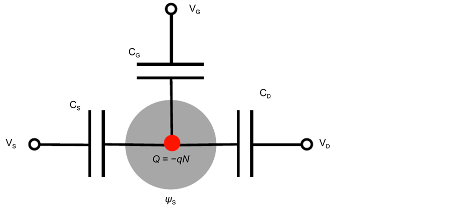
Figure 3. Capacitance models in nano-MOSFET device.

From [12] , subthreshold swing S = 75 mV/V and drain induced barrier lowering DIBL = 80 mV/dec. So, CG, CS and CD can be calculated.
Total Capacitance of NOT gate = Gate Capacitance + Source Capacitance + Drain Capacitance + Area Capacitance + Sidewall Capacitance.
Rise time constant  gate total capacitance.
Rise time , it takes 6.1 times duration to pass logic 1 than logic 0 through an n-channel MOS pass-transistor.
Fall time constant  gate total capacitance.
Fall time 
Propagation delay 
Maximum signal frequency 
3. Results and Discussion
Figure 4 shows the energy sub-band profile along the channel for nano-MOSFET studied in this paper. Drain-to-source voltage, VDS lowers the sub-band potential at the drain side by 0.60 eV [13] [14] [15] .
From Equation (3), the backscattering mean free path is

From Equation (5), the critical length is

From Equation (1), the backscattering coefficient is

From Equation (2), the ballistic efficiency is

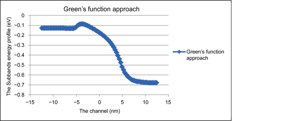
Figure 4. The sub-band energy profile along the channel for Nano-MOSFET.
In order to analyze the NanoMOS simulation result of Figure 5, Equation (10) and Equation (11) are needed. Take VDS = 0.60 V.
Then, by using Equation (10),

After considering the ballistic efficiency B and using Equation (11),

Simulated result with NanoMOS, as in Figure 5, has  From theoretical calculation of Equation (11),
  These two results are
87.3% closely matched. In Figure 5, drain current in saturation region is sloping because electron scattering is considered in Figure 5 and at high drain bias, scattering model in nano-MOSFET exhibits drain current closer to the ballistic limit than under low drain bias.
At region above threshold, the Fermi-Dirac integrals in Equation (11) can be simplified to exponential terms as in equation below.
 (19)
(19)
Sub-band potential at drain side is lower by , therefore

Then Equation (19) becomes
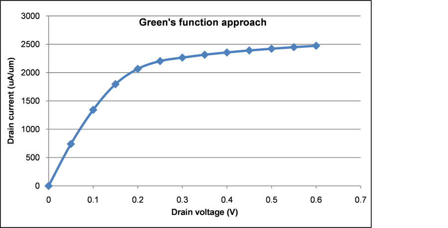
Figure 5. Drain current versus drain voltage for nano-MOSFET by NanoMOS simulation.
 (20)
(20)
After analysis, Equation (19) and Equation (20) both has the same value.

To implement transistor level NOT gate circuit as in Figure 2, the nano-MOSFET should operate in the linear region which is the region for digital logic operation. From Figure 5, linear region is from VDS = 0.00 V until 0.20 V. Use Equation (11) to calculate the drain current at this linear region and then apply Equation (17) to calculate RLoad at quasi-ballistic limit. From Equation (11),

In order to calculate the resistance of nano-MOSFET at quasi-ballistic limit, use Equation (17) since digital logic gates operate at linear portion of I-V curve. Using Vth =
0.20 V,  and from device dimension W = 125 nm, RLoad = 748.8
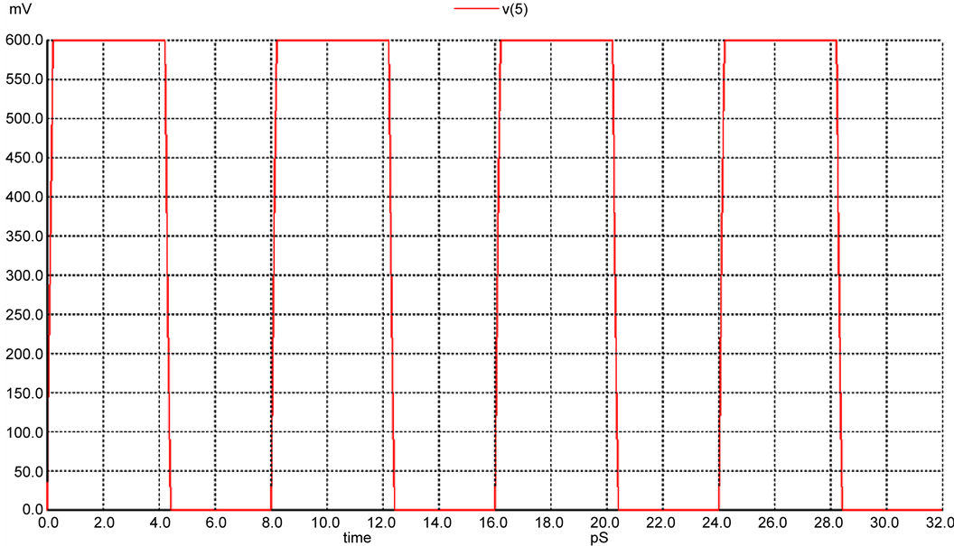
Ω. The resistance value is used in analyzing theoretical value of rise time in NOT gate circuit. On the other hand Equation (18) is used to obtain the resistance needed in analyzing theoretical value of fall time in NOT gate circuit. Finally, the NOT gate circuit in Figure 2 is simulated using WinSpice. The timing diagram result are shown in Figure 6(a) and Figure 6(b).
Low output voltage VOL of NOT transistor level circuit in Figure 2 is given by
 (21)
(21)
From WinSpice simulation timing diagram Figure 6(b),
 (22)
(22)
By comparing Equation (21) and Equation (22),

From theoretical modeling and also WinSpice simulation, VOH = 0.4 V. Nano- MOSFET at the bottom is at off state and thereby at high impedance state. Threshold voltage lost 0.20 V occurs at top side nano-MOSFET load which acts as pass transistor.
Table 2 tabulates the result of this investigation. The theoretical and simulated result are almost matched each other.
4. Conclusion
Modern MOSFET semiconductor devices operate in quasi-ballistic transport. Quasi- ballistic transport is the carrier transport between drift-diffusion and ballistic regimes.
 (a)
(a)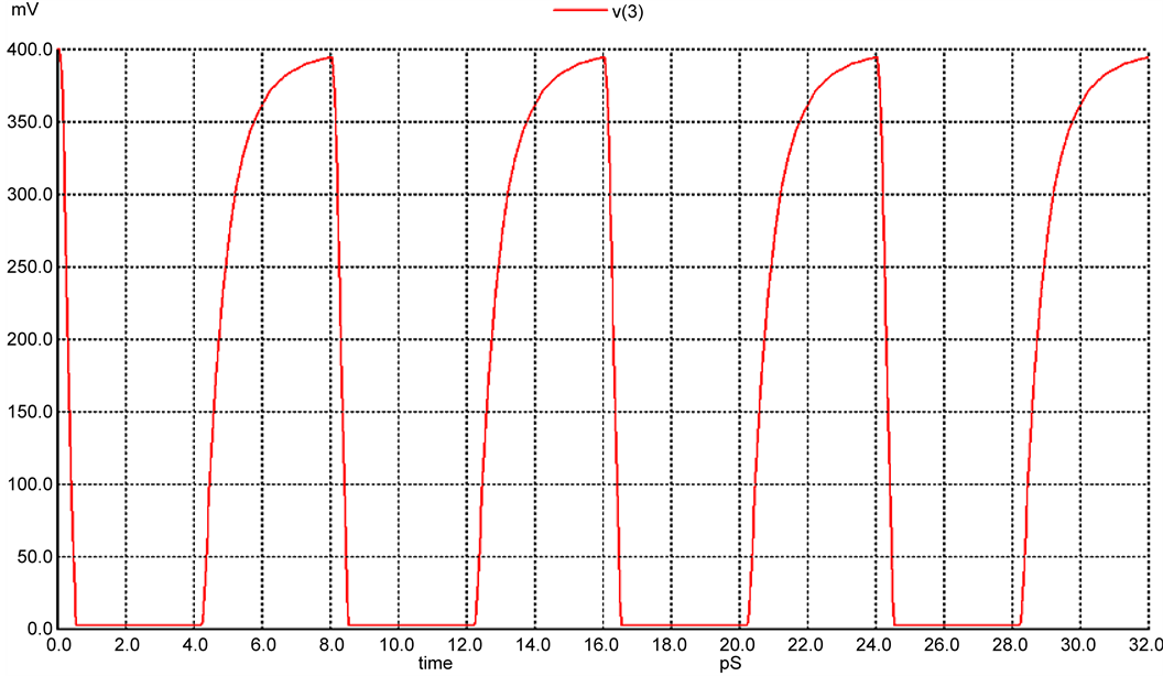 (b)
(b)
Figure 6. (a). WinSpice input signal with period 8 ps to NOT gate; (b) WinSpice output signal of NOT gate.
Table 2. Theoretical and simulated result comparison table.
Theoretical calculations and simulation results about this transport have been done in this paper and this paper shows that theoretical calculation values and simulation results are closely matched. Logic NOT circuit level has been implemented using nano- MOSFET and correct logical operation has been achieved.
Cite this paper
Ooi, C.Y. and Lim, S.K. (2016) Study of Timing Characteristics of NOT Gate Transistor Level Circuit Implemented Using Nano-MOSFET by Analyzing Sub-Band Potential Energy Profile and Current-Voltage Characteristic of Quasi-Ballistic Transport. World Journal of Nano Science and Engineering, 6, 177-188. http://dx.doi.org/10.4236/wjnse.2016.64016
References
- 1. Hosseini, R. and Teimuorzadeh, N. (2013) Simulation Study of Circuit Performance of GAA Silicon Nanowire Transistor and DG MOSFET. Physical Review & Research International, 3, 568-576.
- 2. Gowri Sankar, P.A. and Udhayakumar, K. (2014) MOSFET-Like CNFET Based Logic Gate Library for Low-Power Application: A Comparative Study. Journal of Semiconductors, 35, Article ID: 075001.
https://doi.org/10.1088/1674-4926/35/7/075001 - 3. Wulf, U., Krah-lisch, M. and Richter, H. (2011) Scaling Properties of Ballistic Nano-Transistors. Nanoscale Research Letters, 6, 365.
https://doi.org/10.1186/1556-276X-6-365 - 4. Baldo, M. (2011) Introduction to Nanoelectronics. MIT Open Course Ware Publication, May.
- 5. Navi, K., Rashtian, M., Khatir, A., Keshavarzian, P. and Hashemipour, O. (2010) High Speed Capacitor-Inverter Based Carbon Nanotube Full Adder. Nanoscale Research Letters, 5, 859-862.
https://doi.org/10.1007/s11671-010-9575-4 - 6. Tan, M.L.P., Lentaris, G. and Amaratunga, G.A.J. (2012) Device and Circuit-Level Performance of Carbon Nanotube Field-Effect Transistor with Benchmarking against a Nano-MOSFET. Nanoscale Research Letters, 7, 467.
https://doi.org/10.1186/1556-276X-7-467 - 7. Chin, H.C., Lim, C.S., Wong, W.S. and Tan, M.L.P. (2014) Enhanced Device and Circuit-Level Performance Benchmarking of Graphenenanoribbon Field-Effect Transistor against a Nano-MOSFET with Interconnects. Journal of Nanomaterials, 2014, Article ID: 879813.
https://doi.org/10.1155/2014/879813 - 8. Gupta, R., Tutuianu, B. and Pileggi, L.T. (1997) The Elmore Delay as a Bound for RC Trees with Generalized Input Signals. IEEE Transactions on Computer-Aided Design of Integrated Circuits and Systems, 16, 95-104.
https://doi.org/10.1109/43.559334 - 9. Li, Y.M. and Hwang, C.-H. (2008) High-Frequency Characteristic Fluctuations of Nano-MOSFET Circuit Induced by Random Dopants. IEEE Transactions on Microwave Theory and Techniques, 56, 2726-2733.
https://doi.org/10.1109/TMTT.2008.2007077 - 10. Han, M.-H., Li, Y.M. and Hwang, C.-H. (2010) The Impact of High-Frequency Charactersitics Induced by Intrinsic Parameter Fluctuations in Nano-MOSFET Device and Circuit. Microelectronics Reliability, 50, 657-661.
https://doi.org/10.1016/j.microrel.2010.01.048 - 11. Nasser, A.A.A., Aly, M.H., Abdel Rassoul, R.A. and Khourshed, A. (2011) Performance of Near-Ballistic Limit Carbon Nano-Transistor (CNT) Circuits. ICCTA, 175-182.
- 12. Ren, Z.B. (2011) Nanoscale MOSFETs: Physics, Simulation and Design. PhD Thesis, Purdue University.
- 13. Yee, O.C. and King, L.S. (2015) Simulation Study on the Electrical Performance of Equilibrium Thin-Body Double-Gate Nano-MOSFET. Jurnal Teknologi, 76, 87-95.
- 14. Yee, O.C. and King, L.S. (2016) Simulation Study of 2D Electron Density in Primed and Unprimed Subband Thin-Body Double-Gate Nano-MOSFET of Three Different Thicknesses and Two Temperature States. International Journal of Nanoelectronics and Materials, 9, 67-84.
- 15. Sinha, S.K. and Chaudhury, S. (2012) Simulation and Analysis of Quantum Capacitance in Single-Gate MOSFET, Double-Gate MOSFET and CNTFET Devices for Nanometer Regime. International Conference on Communications, Devices and Intelligent Systems, 28- 29 December 2012.
https://doi.org/10.1109/CODIS.2012.6422160