Modeling and Numerical Simulation of Material Science
Vol.09 No.04(2019), Article ID:95573,11 pages
10.4236/mnsms.2019.94006
Comparative Study of Lead-Free Perovskite Solar Cells Using Different Hole Transporter Materials
Abou Bakary Coulibaly1,2, Sampson Oladapo Oyedele1,2*, N’Guessan Raymond Kre1, Boko Aka1,2
1Université Nangui Abrogoua, UFR des Sciences Fondamentales et Appliquées (SFA), Abidjan, Côte d’Ivoire
2Institut de Recherche sur les Energies Nouvelles (IREN), Abidjan, Côte d’Ivoire
![]()
Copyright © 2019 by author(s) and Scientific Research Publishing Inc.
This work is licensed under the Creative Commons Attribution International License (CC BY 4.0).
http://creativecommons.org/licenses/by/4.0/


Received: July 23, 2019; Accepted: October 6, 2019; Published: October 9, 2019
ABSTRACT
In recent years, there has been an unprecedented rise in the performance of metal halide perovskite solar cells. The lead-free perovskite solar cells (PSCs) have drawn much research interest due to the Pb toxicity of the lead halide perovskite. CH3NH3SnI3 is a viable alternative to CH3NH3PbX3. In this work, we designed a tin-based perovskite simulated model with the novel architecture of (TCO)/buffer (TiO2)/absorber (Perovskite)/hole transport material (HTM) and analyzed using the solar cell capacitance simulator (SCAPS-1D), which is well adapted to study the photovoltaic architectures. In the paper, we studied the influences of perovskite thickness and the doping concentration on the solar cell performance through theoretical analysis and device simulation. The results are indicating that the lead-free CH3NH3SnI3 is having the great potential to be an absorber layer with suitable inorganic hole transport materials like CuI (PCE: 23.25%), Cu2O (PCE: 19.17%), organic hole transport materials like spiro-OMETAD (PCE: 23.76%) and PTAA (PCE: 23.74%) to achieve high efficiency. This simulation model will become a good guide for the fabrication of high efficiency tin-based perovskite solar. The results show that the lead-free CH3NH3SnI3 is a potential environmentally friendly solar cells with high efficiency.
Keywords:
CH3NH3SnI3, SCAPS-1D, Simulator, Perovskite, Thickness, Toxicity, Influence, Efficiency

1. Introduction
Recent global calamities such as floods, rising temperatures have shown the need to use new sources of energy other than fossil fuels. Solar energies are emerging as alternative sources of energy and will play an important role in the years. Solar cells have become one of the most important sources of renewable energy. In recent years, several emerging photovoltaic technologies have shown growing interest in lightness, inexpensive processes and flexibility. Among these technologies, the perovskites with halides appear as a serious candidate to replace the traditional silicon. The organic-inorganic perovskite compounds based on the metal halides adopt the perovskite structure ABX3. This structure consists of an array of shared angle BX6 octahedra, where the B atom is a metal cation (typically Sn2+ or Pb2+) and X is typically F−, Cl−, Br− or I−. The cation A is selected to balance the total charge and it can even be a Cs+ or a small molecular species such as , #Math_3#, ... [1] .
The recent implementation of CH3NH3PbX3 perovskite absorbers (X = I, Cl, Br) with the organic hole conductor 2,2',7,7'-tetrakis (N,N-di-p-methoxyphenylamine) 9,9'-spirobifluorene (OMETAD spiro) has achieved energy conversion efficiencies (PCE) higher than 23% and has been recognized as an emerging revolution in photovoltaic technologies. However, spiro-OMETAD is costly. This is why the development of simple and inexpensive molecular structures is a challenge. In addition, lead in the perovskite sorbent layer has raised serious concerns about the potential impact of the technology on the environment. Lead toxicity problems have been a major barrier to commercial application. There are environmental and human health related complications when lead-based materials are used in perovskite solar cells [2] .
Researchers must focus on achieving a record efficiency of perovskite solar cells (PSC), without overlooking the environmental impact that lead can cause. Lead free-perovskite solar cells will be undeniably crucial if this technology is to be commercialized and to compete with existing photovoltaic technologies. Many device configurations of PSC devices have been proposed to obtain high efficiency with low cost and environmental friendly. Most of the studies is done using lead perovskite material but few studies were done using other perovskite materials and different hole transporter materials (HTM).
Several documents were published on material growth, processing and characterization on one side, and on the performance of finished cells and modules on the other. But interpretation of the experimental data is often difficult. This is due to lack of accurate model and also data about defect, band offsets, carrier density at grain boundaries at interfaces hard to obtain experimentally. Therefore numerical modeling to describe PV thin layer devices is a convenient tool to better understand the basic factors limiting the electrical parameters of the solar cell and to increase their performance [3] . The other advantage is that simulation studies the effect of various parameters on photovoltaic performance without fabricating a solar cell. In this research the simulation device performance is consistent with the experimental value of tin based PSC certifying that the device simulation is valid and the input parameters. Our work is focused on the search for a potential environmentally friendly solar cell with high efficiency and cheaper. So to solve the problem of lead we replaced it with tin in perovskite giving the molecule CH3NH3SnI3. Also, we used cheaper HTM than spiro-OMETAD and compare the performance of the cells obtained with those of lead perovskite with spiro-OMETAD.
2. Methodology
The computer simulation tool employed for our work is SCAPS-1D version 3307 developed by Professor Marc Burgelman [4] . The basic physics supporting SCAPS is the solution of one dimensional general equations for semi conductor based on well know Poisson’s equation, transport equation, continuity equation and taken into account one or several mechanisms of the recombinations. A comprehensive detail of the physics underlying these equations can be found on references.
Poisson’s Equation (1)
Continuity Equation (2)
where Jn = electron current density = the permittivity of the semiconductor
ρ = charge density q = electric charge
Jp = hole current density ρ = charge density
Dn,p = electron, hole diffusion coefficient
µn,p = electron, hole mobility
φ = electrical potential
2.1. The Architecture of Device
The device configuration is one of the most crucial factors for evaluating the performance of perovskite solar cells. The photovoltaic structure studied consist of transparent conductive oxide (TCO)/buffer (TiO2/absorber (perovskite)/hole transporter material (HTM). The cell is illuminated schematically as shown in Figure 1. In this structure the perovskite solar cell has an architecture where the perovskite material is sandwiched between an electron extractor (negative charge carriers) who is TiO2 and a layer extractor of hole (positive charge carriers) the HTM.
2.2. Simulation Details
We enter parameters to definite materials of each layer that compose the solar cell. The input parameters for the simulation study are presented in Table 1. These values are based on experimental results and their references are cited. We have introduced in both interfaces the different parameters shown in Table 2 and for each layer the defect parameters in Table 3. For the optical absorption α (hν), we use combinaison of the six sub-models (back ground, Eg-step, Eg-sqrt, power law 1, power law 2, sub-bandgap) for each layer in order to obtain a better

Figure 1. Architecture device of perovskite.
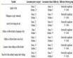
Table 1. Simulation parameters of perovskite solar cells.
Table 2. Interface defect properties panel.
Table 3. Defect properties panel.
result. When we set all these parameters of each layer we launch scaps.
At first we varied the thickness from 100 nm to 1000 nm of perovskite keeping the other parameters invariable. Then we varied the doping concentration of perovskite from 1010 cm−3 to 1018 cm−3. For each simulation four photovoltaic parameters are displayed: the open-circuit voltage (Voc), the current density (Jsc), the fill factor (FF) and the power conversion efficiency (PCE). The curves are plotted with these results to evaluate the performance of the cell (Figure 3, Figure 4).
· Current density (Jsc)
The short-circuit current (Jsc) is the maximum current flowing through the solar cell, i.e. when the cell is short-circuited without load. The highest Jsc corresponds to the zero voltage of the circuit as shown in the graphical representation of short circuit current given in Figure 2 [5] .
· Open circuit voltage (Voc)
The open circuit voltage (Voc) is the maximum voltage measured from a solar cell. When the cell is in open circuit, no current flows then the voltage at its terminals is Voc as shown in Figure 2 [5] .
· Fill factor (FF)
FF is the quality measure for solar cell performance by taking the ratio of maximum power delivered by a solar cell to the theoretical power of a solar cell. Fill factor can also be interpreted as the ratio of rectangular areas depicted in Figure 2 for maximum power point and (MPP) and theoretical maximum power . Fill factor is defined in Equation (3) [5] .
(3)
where Vmp and Jmp are the maximum point voltage and current density generated by a solar cell.
· Power Conversion Efficiency (PCE)
Power Conversion efficiency (PCE) expressed as a percentage is the ratio of the maximum power delivered by the PV cell and the incident light power (Pin) [5] .
PCE is defined in Equation (4).
(4)
![]()
Figure 2. Short circuit current and open circuit voltage representation.
3. Results and Discussion
3.1. Influence of Absorber Layer Thickness on Solar Cell Characteristics
As absorber layer, perovskite plays a critical part to cell performance. The thickness of absorber is one of the most crucial parameters and has remarkable influence on the device. In the simulation, we focus on device performance parameters (i.e. Jsc, Voc, FF and PCE) as a function of absorber thickness (varying from 100 to 1000 nm).
To absorb the maximum number of photons and generate electronn-hole pair, absorber layer should set for optimum thickness. So performance solar cell depends mainly on thickness of absorber layer [14] . Illumination spectrum is global AM 1.5 and operation temperature is 300 K. We keep the dopant concentration to Na = 1015 cm−3 and thicknesses of all HTM to 50 nm, their dopant concentration to Na = 1020 cm−3. We do the simulation with six holes transporting materials (HTM): three inorganics and three organics. The HTM used are 2,2',7,7'-tetrakis-(N,N-di-p-methoxyphenylamine), 9,9'-spirobifluorene (spiro-OMETAD), poly(3-hexylthiophène-2,5diyl(P3HT), copper (I) oxide (Cu2O), poly(triarylamine) (PTAA), nickel oxide (NiO), copper iodide (CuI).
The graphs presented in Figures 3(a)-(d) show respectively the variations of open-circuit voltage (Voc), short circuit current (Jsc), fill factor (FF) and efficiency (PCE) of different holes transporting layers (HTM) with the thicknesses of the absorber layer.
The Voc plots of all HTM used are similar. The simulated result show that with increasing the absorber thickness, Voc values continously increase by varying the thickness from 100 nm to 1000 nm (Figure 3(a)). The best Voc values of each HTM are summarized in Table 4. These values are greater than that of silicon (0.6 v) for all HTMs except for the case of NiO (0.55 v).
Let us analyze the plots of Jsc and PCE (Figure 3(c) & Figure 3(d)). The plots Jsc and PCE are almost similar. It is found that with spiro-OMETAD, CuI and
![]()
Figure 3. Variation of Voc (a), Jsc (b), FF (c), PCE (d) with thickness for each HTM.
Table 4. Simulation results of solar cell performance for each HTM with thickness variation.
PTAA the increase of thickness leads to an increase of the values of Jsc and PCE of the cell. The highest values of Jsc and PCE obtained with these HTM correspond to the largest thickness (1000 nm); spiro-OMETAD (Jsc: 40.05 mA/cm2, PCE: 23.76%); PTAA (Jsc: 40.03 mA/cm2, PCE: 23.58%); CuI (Jsc: 37.15 mA/cm2, PCE: 18.6%).
With HTM P3HT, Cu2O and NiO when we increase the thickness the values of Jsc and PCE increase to an optimal value before dropping. Thus the optimum thickness is 200 nm for P3HT (Jsc: 32.23 mA/cm2, PCE: 17.98%) and NiO (Jsc: 31.45 mA/cm2, PCE: 12.41%). For Cu2O, the optimal thickness is reached at 300nm with Jsc: 32.06 mA/cm2, PCE: 17.91%.
By increasing thickness, the short circuit current (Jsc) increases because a thicker absorber layer will absorb more photons, which will create more electron-hole pair. But with a thicker absorbing layer, the chances of recombination also increase because the charges have to travel a greater distance for diffusion. Therefore, after a certain point, the efficiency decreases with increasing thickness. With increasing thickness, recombination multiplies [10] .
A thinner absorbent layer results in less electron-hole recombination. A thinner absorber layer can produce a higher power conversion efficiency (PCE) than a thicker layer e.g. P3HT, NiO, Cu2O layers (Figure 3(d)).
Fill Factor is considered as an ability to deliver available power a load generated by a cell, in another word, the internal power depletion. In thicker absorbers the internal power depletion enhances and reduces the fill factor. Fill factor is observed maximum value for 100 nm thickness (P3HT: 75.05%, PTAA: 74.14%, Cu2O: 73.87%, NiO: 71.84%, CuI: 77.02%) and for 200 nm (spiro-OMETAD: 70.82%).
The simulation results show us that the highest efficiencies are reached with spiro-OMETAD: 23.76%, PTAA: 23.58% (Table 4). The results suggest that an optimal thickness of 200 nm for absorber layer could result in high efficiency tin perovskite solar cells with P3HT, 300 nm with NiO or Cu2O. If the absorber thickness surpasses the optimal value, it results in more excess carriers and more traps which give more opportunity for occurrence of recombination. For spiro-OMETAD and PTAA the simulation indicates that the optimal thickness is more than 1000 nm.
3.2. Influence of Doping Concentration of Absorber Layer on Solar Cell Characters
Doping is a very important process used to improve the properties of semiconductors devices, such as photovoltaic [15] . Doping of a photoactive material in the solar cell architecture decides the electrical behavior of the layers which will affect the performance of the device [16] .
The dopant concentrations of perovskite were varied from 1010 to 1018 cm−3 in order to identify their effect toward solar cell performances with various HTM. Others parameters are kept constant such as perovskite thickness to 300 nm, all HTM thickness to 50 nm, their doping concentration to Na = 1020 cm−3, temperature to 300 K.
Figure 4 below shows the dependences of Jsc, FF, Voc, and efficiency on dopant concentration. At low dopant concentration (1010 cm−3 < Na < 1014 cm−3), the solar cell parameters almost do not depend on doping. From 1015 cm−3 to 1018 cm−3 a drop of less than 10% of Voc is noted. From 1014 cm−3 to 1016 cm−3, observe an increase of less than 10% of the Jsc, values for all HTMs, then a fall of more than 50% of all these values.
The concentration of 1015 cm−3 represents the optimum value to reach the hightest performance with spiro-OMETAD, and PTAA while Cu2O, P3HT, CuI, NiO requires a concentration of 1016 cm−3. These values are summarized in Table 5 below.
From 1014 cm−3 to 1016 cm−3, the increase of 10% of the Jsc revealed is offset by the drop of 10% in Voc. PCE increases around 10% to reach a maximum value at 1015 cm−3 for spiro-OMETAD and PTAA then at 1016 cm−3 for the other HTMs. After these maximum values occur a fall of more than 30% of PCE is recorded.
It can then be said that increasing the doping concentration to 1014 cm−3 has no effect on cell performance. This behavior of the cell can be explained by a defect growth such as the recombinations that cancel the new charges created. After this concentration value, the number of photogenerated charges accumulates
![]()
Figure 4. Variation of Voc (e), Jsc (f), FF (g), PCE (h) with Na for each HTM.
Table 5. Simulation results of solar cell performance for each HTM with NA variation.
Table 6. Simulation results of solar cell performance for each HTM.
and dominates the defects that appear in the cell, which improves the performance of the cell. This improvement evolved to a concentration of 1015 cm−3 or 1016 cm−3 where the recombination defects take precedence over the created charges. From this moment, a deterioration of the performance of the cell is noted. The best values obtained by our simulation for each HTM used are shown in Table 5.
To better understand the performance of the cells thus formed, we fixed doping concentration constant 1010, 1011, 1012... 1018 cm−3 and we vary the thickness from 100 nm to 1000 nm. The best results are co-signed in Table 6. With HTM PTAA (PCE: 23.74%), CuI (PCE: 23.25%) performance results are obtained similar to those of spiro-OMETAD (PCE: 23.76%).
4. Conclusion
The current quest for the best performance of perovskite solar cells is the subject of many researches and publications. The challenge is to remove some of the barriers that prevent the large-scale marketing of perovskite solar cells, namely the presence of lead, stability and the cost of the cell. We think, we have solved two obstacles: the replacement of lead by tin in perovskite and the reduction of the cost of the cell by using hole transporter materials such as Cu2O, P3HT, CuI cheaper than spiro-OMETAD usually. Furthermore, the results of our simulations showed high efficiencies similar to those of the lead perovskite cell with spiro-OMETAD. However, care must be taken to prevent or reduce the oxidation of Sn2+ to Sn4+ by adding SnF2 during of perovskite synthesis because this reaction favors its rapid degradation.
Acknowledgements
The authors are grateful to Prof Marc Burgelman and colleagues at the University of Gent for providing the SCAPS-1D software reported in this document.
Conflicts of Interest
The authors declare no conflicts of interest regarding the publication of this paper.
Cite this paper
Coulibaly, A.B., Oyedele, S.O., Kre, N.R. and Aka, B. (2019) Comparative Study of Lead-Free Perovskite Solar Cells Using Different Hole Transporter Materials. Modeling and Numerical Simulation of Material Science, 9, 97-107. https://doi.org/10.4236/mnsms.2019.94006
References
- 1. Borriello, I., Cantele, G. and Ninno, D. (2008) Ab Initio Investigation of Hybrid Organic-Inorganic Perovskites Based on Tin Halides. Physical Review B, 77, Article ID: 235214. https://doi.org/10.1103/PhysRevB.77.235214
- 2. Babayigit, A., Boyen, H. and Conings, B. (2018) Environment versus Sustainable Energy: The Case of Lead Halide Perovskite-Based Solar Cells. MRS Energy & Sustainability, 5, E1.https://doi.org/10.1557/mre.2017.17
- 3. Oyedele, S.O. and Aka, B. (2017) Numerical Simulation and Performance Optimization of Cu(In,Ga)Se2 Solar Cells. IOSR Journal of Applied Physics, 8, 1-11.
- 4. Noel, N.K., Stranks, S.D., Abate, A., Wehrenfennig, C., Guarnera, S., Haghighirad, A.A. and Sadhanala, A., et al. (2014) Lead-Free Organic-Inorganic Tin Halide Perovskites for Photovoltaic Applications. Energy & Environmental Science, 7, 3061-3068. https://doi.org/10.1039/C4EE01076K
- 5. Soucase, B.M. (2019) Numerical Analysis for Efficiency Enhancement of Thin Film Solar Cells.
- 6. Du, H.-J., Wang, W.-C. and Zhu J.-Z. (2016) Device Simulation of Lead-Free CH3NH3SnI3 Perovskite Solar Cells with High Efficiency. Chinese Physics B, 25, Article ID: 108803. https://doi.org/10.1088/1674-1056/25/10/108802
- 7. Stoumpos, C.C., Malliakas, C.D. and Kanatzidis, M.G. (2013) Semiconducting Tin and Lead Iodide Perovskites with Organic Cations: Phase Transitions, High Mobilities, and Near-Infrared Photoluminescent Properties. Inorganic Chemistry, 52, 9019-9038. https://doi.org/10.1021/ic401215x
- 8. Kour, N., Mehra, R. and Chandni (2017) Comparative Study of Solar Cell Devices using Lead and Tin based Perovskite Material through Numerical Simulation. International Journal for Scientific Research & Development, 5, 1289-1292.
- 9. Mandadapu, U., Vedanayakam, V., Thyagarajan, K., Reddy, M.R. and Babu, B.J. (2017) Design and Simulation of High Efficiency Tin Halide Perovskite Solar Cell. International Journal of Renewable Energy Research, 7, 1603-1612.
- 10. Haider, S.Z., Anwar, H. and Wang, M.Q. (2018) A Comprehensive Device Modelling of Perovskite Solar Cell with Inorganic Copper Iodide as Hole Transport Material. Semiconductor Science and Technology, 33, Article ID: 035001. https://doi.org/10.1088/1361-6641/aaa596
- 11. Intaniwet, A., Mills, C.A., Sellin, P.J., Shkunov, M. and Keddie, J.L. (2010) Achieving a Stable Time Response in Polymeric Radiation Sensors under ChargeInjection by X-Rays. ACS Applied Materials & Interfaces, 2, 1692-1699.
- 12. Karimi, E. and Ghorashi, S.M.B. (2017) Simulation of Perovskite Solar Cell with P3HT Hole-Transporting Materials. University of Kashan, Atomic and Molecular Group, Faculty of Physics, Kashan, Iran. https://doi.org/10.1117/1.JNP.11.032510
- 13. Casas, G.A., Cappelletti, M.A., Cédola, A.P., Soucase, B.M. and Peltzer, E.L. (2017) Analysis of the Power Conversion Efficiency of Perovskite Solar Cells with Different Materials as Hole-Transport Layer by Numerical Simulations. Superlattices and Microstructures, 107, 136-143. https://doi.org/10.1016/j.spmi.2017.04.007
- 14. Soucase, B.M., Pradas, I.G. and Adhikari, K.R. (2016) Numerical Simulations on Perovskite Photovoltaic Devices. In: Pan, L.K. and Zhu, G., Eds., Perovskite Materials: Synthesis, Characterisation, Properties, and Applications, IntechOpen, London, 22.
- 15. Stella, M. (2009) Study of Organic Semiconductors for Device Applications. Thesis, 34-36.
- 16. Mandadapu, U., Victor Vedanayakam, S. and Thyagarajan, K. (2017) Simulation and Analysis of Lead Based Perovskite Solar Cell Using SCAPS-1D. Indian Journal of Science and Technology, 10, 1-8. https://doi.org/10.17485/ijst/2017/v10i11/110721