Open Journal of Inorganic Non-metallic Materials
Vol. 2 No. 4 (2012) , Article ID: 23428 , 4 pages DOI:10.4236/ojinm.2012.24006
Nanoparticles Deposition at Specific Sites Using Aligned Fiber Networks
1Multi-disciplinary Materials Research Center, Frontier Institute of Science and Technology, Xi’an Jiaotong University, Xi’an, China
2Department of Materials Science and Engineering, Virginia Tech, Blacksburg, USA
3Engineering Science and Mechanics, Virginia Tech, Blacksburg, USA
4Department of Mechanical Engineering, Virginia Tech, Blacksburg, USA
Email: *yaodongy@mail.xjtu.edu.cn, *nain@vt.edu
Received July 6, 2012; revised August 11, 2012; accepted September 6, 2012
Keywords: Nanoparticles; Functional Materials; Fibre Technology
ABSTRACT
We report a new method to precisely locate inorganic nanoparticles at polymeric fiber crossing sites. Polymeric fibers are aligned by a previously reported non-electrospinning Spinneret based Tunable Engineered Parameters (STEP) polymeric fiber manufacturing technique. Cross-hatch pattern (perpendicular) of polymeric fibers embedded with inorganic nanoparticles (e.g. Fe(NO3)3 or Bi(NO3)3) were fabricated on top of each other and the fiber compositions reacted during annealing process, thus, producing a desired phase (e.g. BiFeO3) only at the crossing site. Our method offers an easy way to mass arrange and locate nanoparticles at designed positions on virtually all types of substrates.
1. Introduction
Nanomaterials have attracted much interest because of their novel properties compared to bulk materials [1,2]. Different manufacturing processes such as sol-gel [3], solid state reaction [4], and hydrothermal method [5] have been widely used to synthesize nanomaterials. Synthesis is typically followed by application of nanomaterials in engineering, which is currently limited due to difficulties in spatial organization and deposition of nanomaterials. The two main approaches to deposit nanomaterials in a controllable way are through self-assembly [6] and engineered assembly via vapor phase synthesis on top of a seed layer [7,8]. For example, with the help of a focused ion beam (FIB), a method to pattern BaTiO3 thin films have been demonstrated via pulsed laser deposition [7]. Buhlmann et al. also reported the growth of Pb(Zr,Ti)O3 single crystals on TiO2 seeds via sputtering [9].
In this work, we report an alternative and simple way to achieve patterning of nanomaterials. Spinneret based Tunable Engineered Parameters (STEP) non-electrospinning fiber manufacturing platform has recently been developed to deposit polymeric nano/microfibers [10,11]. This technique can continuously deposit uniform diameter micro/nano polymer fibers with control on fiber dimensions (diameter: sub 100 nm—microns, length: mmcm, orientation: parallel and orthogonal) in single and multiple layers at user defined spacing. Furthermore, STEP allows deposition of single and multiple-layer fibrous structures in planar, and customized three-dimensional configurations. These polymer networks can be used as inorganic nanomaterial carriers, through mixing of metal oxide ion solutions with polymer solutions before spinning. Post fiber fabrication, the networks are subjected to high heat, which ablates the base polymer and initiates a chemical reaction at intersection of two or more different types of fibers, thus, resulting in the formation of a new phase only at specific locations.
2. Materials and Methods
2.1. Materials
Two different polymer solutions: polystyrene (PS) (Mw = 2,257,000, Scientific Polymer, USA) dissolved in Xylene at 7 wt%; and polyvinylpyrrolidone (PVP) (SigmaAldrich, USA) dissolved in a mixture solvent (6 ml ethyl alcohol and 5 ml H2O) at 6 wt% were used in this study. A metal source of 0.202 g Fe(NO3)3·9H2O or 0.243 g Bi(NO3)3·5H2O was added into PVP solution.
2.2. Fiber Deposition
The solution was pumped through the micropipette at a flow rate of 20 ml/hour using a syringe pump (Fisher Scientific Inc, USA). STEP based resultant fibers were collected on the substrate (4 - 8 mm in width) in aligned configurations at 1000 RPM and cris-cross structures were fabricated by depositing fibers on top of previously deposited layers. SrTiO3 signal crystal substrates were used to collect fibers.
2.3. Characterization
Scanning electron microscopy (SEM) images were obtained using a LEO (Zeiss) 1550 high-performance Schottky field-emission SEM operated at 5 kV. Oxford INCA Energy E2H X-ray Energy Dispersive Spectrometer (EDS) system with Silicon Drifted detector attached to SEM was used to take DES data. A FEI Helios 600 NanoLab focused ion beam SEM or FIB was used to lift-out transmission electron microscope (TEM) samples. A Philips EM420 transmission electron microscope was then used to obtain cross sectional images.
3. Results and Discussion
The STEP technique offers a simple and cost-effective way, to spin aligned polymer fibers with well-controlled separation distances. Smooth and uniform diameter 500 nm diameter parallel PS fibers were deposited at 2 microns separation distances (Figure 1(b)). Metal oxide ion solution was then mixed into the PVP polymer precursor as mentioned above and using STEP fibers were deposited at precise locations and annealed to obtain pure oxide fibers. Figure 1(c) provides an example of PVP-Fe+ fibers post annealing with tunable and well-controlled distances between two fibers. The aligned fiber structures were observed to possess strong anisotropy, as evidenced by the decreased contact angle along the fiber axis. Water droplets spread easily along the aligned PS fibers and are observed to sit on (001) oriented SrTiO3 substrates on which fibers were deposited (data not shown).
Figure 2(a) shows a schematic of the process by which nanoparticles were located. After obtaining two layers of metal ion-PVP fibers, the fibers were annealed at 700˚C for 1 h, leading to polymer material being burnt off completely, thus, forming the metal oxide. At the intersection of two fibers, the two different metal based particles chemically reacted and produced a new oxide phase of BiFeO3 (Figures 2(b) and (c)). Melting of polymer together with the dispersed metal ions happens between two fibers and the annealed fibers (300 nm in diameter) are thinner than the original polymer fibers. Please note that the oxide fibers maintained good alignment at the crossing of fibers, as clearly can be seen in the image of Figure 2(e).
Since only the intersection regions have both Bi and Fe elements, EDS line scans were used to confirm the
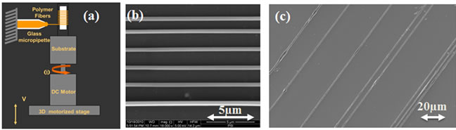
Figure 1. (a) Schematic representation of STEP setup; (b) evenly spaced PS fibers; and (c) well aligned PVP-Fe+ fibers with different spacing.

Figure 2. (a) Schematic map of the proccess of using crossings of oxide fibers to locate oxide nanoparticles. SEM images with different maginfication of as-spun fibers (b) and (d) and annealed fibers (c) and (e).
elemental ratio of the reactant phase in the fibers. Three such line scans were taken from different fiber cross sections as shown in Figure 3(a). The EDS line scans from these three different areas (line scan areas are marked in Figure 3(a)) are shown in Figure 3 for Fe (parts b, d, f) and Bi elements (parts c, e, g). EDS plots confirmed the fiber along y axis has higher concentration of element Fe (part b, c) and along x axis has higher concentration of element Bi (part d, e), whereas at the regions of intersecttion fibers both Bi and Fe elements were found, leading to formation of BiFeO3.
To further study the fiber intersection regions, we used a FIB to lift-out annealed fiber cross section areas and obtain cross sectional images using transmission electron microscope (TEM). TEM samples were made by liftingout regions shown as broken line in Figure 2(e). Figure 4(a) shows top (Fe abundant), middle (both Bi, Fe abundant), and bottom (Bi abundant) at the cross section. Figures 4(b), (c) and (d) show corresponding images at higher magnification of each region. Figures 4(b) and (c) clearly demonstrate 10nm particles aggregating together. Interestingly, these aggregated regions are aligned along the fiber axis in both top and bottom fibers and are attributed to form during the fiber spinning process. Please note that there are many holes in both top and bottom fibers, because during annealing polymer burned out and
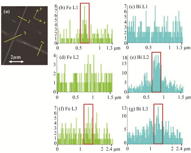
Figure 3. EDS line scans of elemental distribution across fibers. (a) SEM image of the entire area studied from where EDS line scans were obtained, the line scanned areas are marked with numbers. (b) and (c) scan profiles taken from the line marked as “1” in a; (d) and (e) scan profiles taken from the line marked as “2”; (f) and (g) scan profiles taken from the line marked as “3”; (b), (d) and (f) are profiles for Fe element; (c), (e) and (g) are these for Bi element.

Figure 4. TEM images of fiber intersection regions. (a) Figure area studied including Bi, BiFeO3, and Fe based nanoparticles; (b), (c) and (d) Higher resolution images taken from Bi, Fe, and Fe-Bi boundary regions. Insert in (d) shows a selected area electron diffraction pattern from Bi-Fe region.
left some spaces. A high resolution image of the middle reveals denser region, with fewer holes. The contrast in Figure 4(d) is attributed to different BiFeO3 nanograins. The inset shows selected area diffraction pattern, which is consistent with the reflections and positions of the BiFeO3 structures and the rings show BiFeO3 is polycrystalline and well crystalized.
4. Conclusion
In conclusion, an application to locate nanoparticles using STEP platform has been demonstrated based on a fiber-fiber intertexture composite construction. EDS and TEM were used to study and analyze fiber intersection regions. It is an easy and inexpensive way by which to locate nanoparticles at preferred spatial positions. Compared to these vapor deposition methods our method just costs approximately 10%. Though this study demonstrates fibers as carriers of two inorganic nanomaterials in the network, it is easily expandable to accommodate multiple fiber types of different diameters and carriers in the same network, thus leading to complex patterns and arrangements of fused nanomaterials at desired locations in planar and nonplanar sites for applications ranging from advanced materials to sensor systems.
5. Acknowledgements
The authors gratefully acknowledge the financial support from the Ministry of Science and Technology of China through a 973-Project under Grant No.2012CB619401 and National Science Foundation (USA) under DMR- 0757502. The authors are also thankful to Institute for Critical Technology and Applied Sciences (ICTAS) along with Nanoscale Characterization and Fabrication Laboratory (NCFL) at Virginia Tech for SEM and TEM work.
REFERENCES
- L. Yan, Y. D. Yang, Z. G. Wang, Z. P. Xing, J. F. Li, and D. Viehland, “Review of Magnetoelectric Perovskite-Spinel Self-Assembled Nano-Composite Thin Films,” Journal of Materials Science, Vol. 44, No. 19, 2009, pp. 5080-5094. doi:10.1007/s10853-009-3679-1
- Y. D. Yang, L. T. Qu, L. M. Dai, T. S. Kang and M. Durstock, “Electrophoresis Coating of Titanium Dioxide on Aligned Carbon Nanotubes for Controlled Syntheses of Photoelectronic Nanomaterials,” Advanced Materials, Vol. 19, No. 9, 2007, pp. 1239-1243. doi:10.1002/adma.200602181
- J. Y. Fan and P. K. Chu, “Group IV Nanoparticles: Synthesis, Properties, and Biological Applications,” Small, Vol. 6, No.19, 2010, pp. 2080-2098. doi:10.1002/smll.201000543
- Y. D. Yang, S. Priya, J. F. Li and D. Viehland, “TwoPhase Coexistence in Single-Grain BaTiO3-(Mn0.5Zn0.5) Fe2O4 Composites, Via Solid-State Reaction,” Journal of the American Ceramic Society, Vol. 92, No. 7, 2009, pp. 1552-1555. doi:10.1111/j.1551-2916.2009.03068.x
- S. Zhou, X. D. Fang, Z. H. Deng and D. Li, “Preparation of Delafossite-Type Oxides by Hydrothermal Method,” Progress in Chemistry, Vol. 22, No. 2-3, 2010, pp. 352-357.
- Y. Ni, W. F. Rao and A. G. Khachaturyan, “Pseudospinodal Mode of Decomposition in Films and Formation of Chessboard-Like Nanostructure,” Nano Letters, Vol. 9, No. 9, 2009, pp. 3275-3281. doi:10.1021/nl901551j
- Y. D. Yang, J. J. Yao, J. F. Li, J. Das and D. Viehland, “Multi-Orientation Patterned Deposition of BaTiO3 Thin Films Using an Au Buffer Layer,” Thin Solid Films, Vol. 518, No. 20, 2010, pp. 5806-5809. doi:10.1016/j.tsf.2010.05.108
- Y. D. Yang, J. J. Yao, Y. U. Wang, J. F. Li, J. Das and D. Viehland, “Interaction of Gold Nanoparticles in Barium Titanate Thin Films,” ACS Nano, Vol. 3, No. 10, 2009, pp. 3045-3050. doi:10.1021/nn9008406
- S. Buhlmann, P. Muralt and S. Von Allmen, “Lithography-Modulated Self-Assembly of Small Ferroelectric Pb(Zr,Ti)O-3 Single Crystals,” Applied Physics Letters, Vol. 84, No. 14, 2004, pp. 2614-2616. doi:10.1063/1.1690873
- A. S. Nain, J. A. Phillippi, M. Sitti, J. MacKrell, P. G. Campbell and C. Amon, “Control of Cell Behavior by Aligned Micro/Nanofibrous Biomaterial Scaffolds Fabricated by Spinneret-Based Tunable Engineered Parameters (STEP) Technique,” Small, Vol. 4, No. 8, 2008, pp. 1153-1159. doi:10.1002/smll.200800101
- A. S. Nain, M. Sitti, A. Jacobson, T. Kowalewski and C. Amon, “Dry Spinning Based Spinneret Based Tunable Engineered Parameters (STEP) Technique for Controlled and Aligned Deposition of Polymeric Nanofibers,” Macromolecular Rapid Communications, Vol. 30, No. 16, 2009, pp. 1406-1412. doi:10.1002/marc.200900204
NOTES
*Corresponding authors.
#Yaodong Yang and Ji Wang contributed equally to this work.