Advances in Materials Physics and Chemistry
Vol.10 No.01(2020), Article ID:97867,9 pages
10.4236/ampc.2020.101002
The Polar Solvent Application Method for Organic Transparent Conductive Film Produced by an Inkjet Printing Method
Atsushi Nitta1*, Naohiko Chosa2, Kazuhiro Takeda3
1Department of Electronic Control Engineering, National Institute of Technology, Kagoshima College, Kirishima, Japan
2Advanced Mechanical and Electronic Systems Engineering, National Institute of Technology, Kagoshima College, Kirishima, Japan
3Department of Information Engineering, National Institute of Technology, Kagoshima College, Kirishima, Japan

Copyright © 2020 by author(s) and Scientific Research Publishing Inc.
This work is licensed under the Creative Commons Attribution International License (CC BY 4.0).
http://creativecommons.org/licenses/by/4.0/


Received: December 5, 2019; Accepted: January 13, 2020; Published: January 16, 2020
ABSTRACT
In recent years, flexible electronic devices have attracted much attention. Accordingly, flexible transparent conductive films are being researched actively. The commonly used indium tin oxide (ITO) transparent conductive film has limited flexibility. Therefore, we focused on poly(3,4-ethylenedioxythio- phene)/poly(styrenesulfonate)(PEDOT:PSS) as a substitute material for ITO and are engaged in producing flexible transparent conductive film using inkjet printers. To improve the characteristics of the transparent conductive film produced by inkjet printing, based on prior research, we found that cleaning the film substrate with ultraviolet/ozone (UV/O3) and post-deposition annealing and treatment using polar solvents are effective for thin films. In this study, we examined the method of applying the polar solvent. As a result, we were able to improve the homogeneity of the thin film surface by applying the polar solvent to each thin film lamination layer. The resulting characteristics obtained for a three-layer printed PEDOT:PSS thin film with polar solvent coating were resistivity of 1.49 × 10⁻³ Ω·cm and transmittance of 84.6%. However, we found that the surface condition changed depending on the processing method, affecting the rate of visible light transmittance.
Keywords:
PEDOT:PSS, Inkjet Printing, Transparent Conductive Film, Flexible Devices

1. Introduction
Recently, there has been a surge of interest in printed electronics, a technique allowing electronic circuits and devices to be created on flexible substrates made from materials such as plastic [1] [2] [3]. Flexible and stretchable devices enable a high degree of freedom in terms of shape and do not break easily. Therefore, flexible solar cells, displays, and sensors are popular areas of research [4] - [9]. In these electronic devices, transparent electrodes, which transmit visible light and possess conductivity, are important components. The transparent conductive film used as a component in these devices is therefore required to be flexible as well. Indium tin oxide (ITO), a transparent conductive film, is typically used; however, because it contains the rare metal indium, it poses challenges of depletion of resources and rapid fluctuation in price. ITO is also unsuitable for flexible devices as it cannot resist a bending force. Research has been conducted on various materials as substitutes for ITO, including organic materials and carbon nanotubes (CNTs) [10] [11] [12] [13] [14]. The practicality of organic materials is starting to be recognized to build organic electroluminescence (EL) displays, organic thin-film solar cells, and organic transistors [15] - [20]. These organic electronics do not require high-temperature vacuum processing; hence, they can be manufactured using low-temperature processes, and devices can be produced inexpensively by printing and coating techniques [21] [22].
In this study, we focused on poly(3,4-ethylenedioxythiophene)/poly(styrene- sulfonate)(PEDOT:PSS), a conductive polymer material with high flexibility and conductivity, as a substitute for ITO. We produced a flexible transparent conductive film by applying the material onto a plastic substrate using an inkjet printer. The main challenges in producing the organic transparent conductive film using the inkjet printing method are homogeneity of the surface and improving the characteristics of the thin film [23]. If we can solve these issues and produce a practical transparent conductive film, it will become possible to manufacture flexible devices, including wiring and electrodes, using only printing technology. So far, we have found that cleaning the substrate with ultraviolet/ozone (UV/O3) and post-deposition annealing and treatment using polar solvents are effective for PEDOT:PSS thin films [24] [25]. The characteristics of the thin film were also improved by changing the ink solvent from ethanol to dimethyl sulfoxide (DMSO). However, because of the surface roughness of each layer, the interface state affected the resistivity [26]. In this study, we investigated the method of applying the polar solvent, ethylene glycol, to the thin film produced using ink containing DMSO, intending to make the thin film more uniform and improve its characteristics.
2. Experimental
2.1. Production of Ink Material for the Transparent Conductive Film
In the present study, CLEVIOS (Clevios™ PH500) was used as PEDOT:PSS. This conductive polymer has excellent electrical conductivity and high transmittance in the visible light spectrum and has attracted attention for its excellent mechanical flexibility. Figure 1 shows the molecular structure of PEDOT:PSS, and Table 1 shows its physical properties.
The nozzle diameter of a commercially available inkjet printer ranges from a few micrometers to a few tens of micrometers; thus, it is possible to use PEDOT:PSS with the inkjet printing method. However, because the viscosity of the ink for inkjet printers is 5 to 15 mPa·s, it is essential to reduce the viscosity of PEDOT:PSS ink. It has been reported that the properties of the PEDOT:PSS thin film are improved by adding additives [27] [28]. For example, adding ethanol reduces the surface tension of the ink and improves the wettability to the substrate. Adding ethylene glycol or DMSO has a secondary doping effect on PEDOT, enhancing the conductivity by combining the conductive regions [29] [30]. Table 2 shows the characteristics of ink additives. We used an ink composition of PEDOT:PSS:DMSO:ethylene glycol = 70:20:10 wt%, which has obtained the lowest resistance in previous research results [26].
2.2. Preparation and Evaluation of the Thin Film
A piezoelectric pigment inkjet printer (PX-105; Seiko Epson CO.) was used to produce the PEDOT:PSS thin film, with the printing pattern set to 40 mm (L) ×

Figure 1. The molecular structure of the PEDOT:PSS.
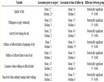
Table 1. Material properties of the PEDOT:PSS.
Table 2. Material properties of the ink additives.
15 mm (W). The substrate used was a heat-resistant transparent film (Teonex Q65-FA; Teijin DuPont Films Co., Ltd.). Q65-FA is a PEN film with excellent thermal stability, chemical resistance, and high transparency. A UV/O3 cleaning process was used to clean the substrate before forming the film (ASM401N; Asumi Giken, Ltd.). Cleaning with UV/O3 reduces organic contaminants on the substrate and improves its hydrophilicity. This treatment improves the electrical properties of the PEDOT:PSS thin film [24]. The conditions for UV/O3 cleaning were a UV irradiation distance of 30 mm, low-pressure mercury lamp output of 40 W, and cleaning time of 20 min. The film was fabricated by applying ink multiple times (double, triple, and quadruple printing). The polar solvent was applied using the printer, with ethylene glycol used as the chemical. The thin film was annealed for 60 min after the entire printing process was completed, using a constant-temperature drying oven (EOP-300B; As One Co., Ltd.). We evaluated the resistivity, transmittance, and surface observation results of the PEDOT:PSS thin film formed. The resistance value was measured using a digital multimeter (VOAC7521H; Iwatsu Electric Co., Ltd.). The thickness of the produced PEDOT:PSS thin film was measured using a stylus-type surface roughness tester (NanoMap-PS; AEP Technology Co.). The film thickness was measured with a multiple incidence angle high-speed spectroscopic ellipsometer (M-2000V-Te; J. A. Woollan Co., Ltd.), which was used together with the resistance value to calculate the resistivity. The transmittance was measured at a wavelength of 550 nm using a spectrophotometer (U-3900; Hitachi High-Technologies Co.). The surface of the thin film was observed under a microscope (VHX-1000; Keyence Co., Ltd.). The surface roughness was measured using an atomic force microscope (AFM) (NaioAFM; Nanosurf Co.).
3. Results and Discussion
Figure 2 shows the change in resistivity when the polar solvent is applied. It has been reported that the resistivity decreases when PEDOT:PSS is evenly distributed [31] [32]. Single or double printing results in an uneven distribution of the ink, while printing several times provides a denser ink distribution, and hence it becomes more uniform. Therefore, the resistivity of the triple-printed ink is lower than that of the double-printed one. However, with four layers of printing, the resistivity increases, which is due to the increase in interfaces when printed multiple times. The film thickness increases as it is printed more times, reaching

Figure 2. Resistivity as a function of the polar solvent application method and the number of printing times.
180 to 185 nm with triple printing. On applying the polar solvent after printing, the resistivity of the PEDOT:PSS thin film did not improve. However, applying the polar solvent to each layer of PEDOT:PSS thin film during printing resulted in reduced resistivity. When a polar solvent was applied to the PEDOT:PSS thin film after each printing, the arrangement of PEDOT molecules in each layer was promoted and the conductivity was considered to be improved. The triple printed film had a resistivity of 1.73 × 10⁻³ Ω·cm, which is the lowest resistivity obtained so far.
Figure 3 shows the visible light transmittance when the polar solvent is applied. Figure 4 shows an image of the thin film surface observed under a microscope. The visible light transmittance decreases when the polar solvent is applied. The microscope image shows that when the polar solvent is applied, the thin film becomes more uniform, with fewer light and dark regions.It has been reported that the visible light transmittance of a uniform thin film without gaps is lower than that of a thin film in an aggregated state [24]. A reason for the reduced transmittance is believed to be the dark blue color of the PEDOT:PSS material, resulting in less light being transmitted when it forms a uniform thin film.
Figure 5 shows the surface roughness of the film, measured using an AFM. The surface roughness increased when the polar solvent was applied. This increase was not observed with ink containing ethanol. This is believed to be because using a printer to apply the polar solvent affected the thin film that had not dried, making the surface rough.
With thin films produced using ink containing DMSO, there was an issue of the surface of the film becoming uneven owing to the rise in viscosity of the ink and the slow drying of the thin film [26]. The thin film was more uneven when the polar solvent was applied. It has been reported that the electrical and optical properties improve if the surface roughness is reduced [23]. However, we were able to prevent the resistivity from increasing. This indicates that it is effective to apply the polar solvent to each layer. The reduction in transmittance suggests that the uneven surface enhances the scattering of light. In the future, further

Figure 3. Transmittance as a function of the polar solvent application method and the number of printing times.

Figure 4. Microscope image of the surface of a PEDOT:PSS (3 times printing, ×100). (a): No polar solvent. (b): Apply polar solvent to the surface. (c): Apply polar solvent to each layer.

Figure 5. AFM image of the surface of a PEDOT:PSS (3 times printing, ×100). (a): No polar solvent. (b): Apply polar solvent to the surface. (c): Apply polar solvent to each layer.
improvements in the homogeneity are required to improve the electrical and optical properties of thin films.
4. Conclusions
The resistivity was reduced by applying the polar solvent to each layer of the PEDOT:PSS thin film during printing. The triple printed film had a resistivity of 1.73 × 10⁻³ Ω·cm, which is the lowest resistivity obtained so far.
Applying the polar solvent rendered the light and dark areas on the film surface more uniform. This is believed to be a factor in the reduction in transmittance.
When the polar solvent was applied using a printer, the thin film surface became more uneven. This is believed to be because applying a polar solvent using a printer affects the thin film, making the surface rougher. Despite the surface of the thin film becoming more uneven, it was possible to improve its conductivity by applying the polar solvent to each layer.
Furthermore, it is necessary to improve the homogeneity of the thin film surface in the future by investigating the method for applying the polar solvent and the chemicals used.
Conflicts of Interest
The authors declare no conflicts of interest regarding the publication of this paper.
Cite this paper
Nitta, A., Chosa, N. and Takeda, K. (2020) The Polar Solvent Application Method for Organic Transparent Conductive Film Produced by an Inkjet Printing Method. Advances in Materials Physics and Chemistry, 10, 17-25. https://doi.org/10.4236/ampc.2020.101002
References
- 1. Sachin, A., Michael, J., Lucian, L. and Lokendra, P. (2018) Cellulose and Nanocellulose-Based Flexible-Hybrid Printed Electronics and Conductive Composites—A Review. Carbohydrate Polymers, 198, 329-336. https://doi.org/10.1016/j.carbpol.2018.06.045
- 2. Stefano, C., Noemi, C., Ilaria, C., Danila, M., Maxim, P., Enrico, S., Reinhard, R.B. and Fabiana, A. (2018) Electroanalysis Moves towards Paper-Based Printed Electronics: Carbon Black Nanomodified Inkjet-Printed Sensor for Ascorbic Acid Detection as a Case Study. Sensors and Actuators B: Chemical, 265, 155-160. https://doi.org/10.1016/j.snb.2018.03.006
- 3. Correia, V., Mitra, K.Y., Castro, H., Rocha, J.G., Sowade, E., Baumann, R.R. and Lanceros-Mendez, S. (2018) Design and Fabrication of Multilayer Inkjet-Printed Passive Components for Printed Electronics Circuit Development. Journal of Manufacturing Processes, 31, 364-371. https://doi.org/10.1016/j.jmapro.2017.11.016
- 4. Christina, K., Alexandros, Z., Christos, K., Evangelos, M., Christoforos, G., Argiris, L. and Stergios, L. (2018) Efficient Flexible Printed Perovskite Solar Cells Based on Lead Acetate Precursor. Solar Energy, 176, 406-411. https://doi.org/10.1016/j.solener.2018.10.055
- 5. Fan, Z.Y., et al. (2018) Experimental Investigation of the Mechanical Robustness of a Commercial Module and Membrane-Printed Functional Layers for Flexible Organic Solar Cells. Composites Part B: Engineering, 147, 69-75. https://doi.org/10.1016/j.compositesb.2018.04.007
- 6. Wei, X.Y., et al. (2019) Fully-Integrated Motion-Driven Electroluminescence Enabled by Triboelectrification for Customized Flexible Display. Nano Energy, 61, 158-164. https://doi.org/10.1016/j.nanoen.2019.04.005
- 7. Wen, B.-J., et al. (2016) Non-Contact Resistance Measurement of Transparent Electrodes Deposited on Flexible Display Substrates under Repetitive Bending Test by Terahertz Time Domain Spectroscopy. Displays, 45, 58-62. https://doi.org/10.1016/j.displa.2016.01.002
- 8. Sato, J., et al. (2019) Ferroelectric Polymer-Based Fully Printed Flexible Strain Rate Sensors and Their Application for Human Motion Capture. Sensors and Actuators A: Physical, 295, 93-98. https://doi.org/10.1016/j.sna.2019.05.022
- 9. Sarfraz, J., et al. (2018) The Performance of Inkjet-Printed Copper Acetate Based Hydrogen Sulfide Gas Sensor on a Flexible Plastic Substrate-Varying Ink Composition and Print Density. Applied Surface Science, 445, 89-96. https://doi.org/10.1016/j.apsusc.2018.03.142
- 10. Fischer, R., et al. (2018) Stable and Highly Conductive Carbon Nanotube Enhanced PEDOT:PSS as Transparent Electrode for Flexible Electronics. Organic Electronics, 62, 351-356. https://doi.org/10.1016/j.orgel.2018.07.022
- 11. Jiang, S., Hou, P.-X., Liu, C. and Cheng, H.-M. (2019) High-Performance Single-Wall Carbon Nanotube Transparent Conductive Films. Journal of Materials Science & Technology, 35, 2447-2462. https://doi.org/10.1016/j.jmst.2019.07.011
- 12. Zhou, B., et al. (2019) Interfacial Adhesion Enhanced Flexible Polycarbonate/Carbon Nanotubes Transparent Conductive Film for Vapor Sensing. Composites Communications, 15, 80-86. https://doi.org/10.1016/j.coco.2019.06.012
- 13. Wen, L., et al. (2019) Study on the Electrical, Optical, Structural, and Morphological Properties of Highly Transparent and Conductive AZO Thin Films Prepared near Room Temperature. Applied Surface Science, 473, 649-656. https://doi.org/10.1016/j.apsusc.2018.11.250
- 14. Li, M.L., Wang, Y.B., Wang, Y. and Wei, X.H. (2017) AZO/Ag/AZO Transparent Flexible Electrodes on Mica Substrates for High Temperature Application. Ceramics International, 43, 15442-15446. https://doi.org/10.1016/j.ceramint.2017.08.089
- 15. Islam, A., et al. (2019) Meta-Substituted Bipolar Imidazole Based Emitter for Efficient Non-Doped Deep Blue Organic Light Emitting Devices with a High Electroluminescence. Journal of Photochemistry and Photobiology A: Chemistry, 379, 72-78. https://doi.org/10.1016/j.jphotochem.2019.04.033
- 16. Shahalizad, A., et al. (2017) Near Infrared Electroluminescence from Nd(TTA)3phen in Solution-Processed Small Molecule Organic Light-Emitting Diodes. Organic Electronics, 44, 50-58. https://doi.org/10.1016/j.orgel.2017.01.044
- 17. Ganesan, S., Mehta, S. and Gupta, D. (2019) Fully Printed Organic Solar Cells—A Review of Techniques, Challenges and Their Solutions. Opto-Electronics Review, 27, 298-320. https://doi.org/10.1016/j.opelre.2019.09.002
- 18. Joodaki, M. and Salari, M. (2018) Investigation of the Tensile Strain Influence on Flicker Noise of Organic Solar Cells under Dark Condition. Organic Electronics, 59, 230-235. https://doi.org/10.1016/j.orgel.2018.05.018
- 19. Al Ruzaiqi, A., et al. (2019) Low-Voltage Organic Thin-Film Transistors Based on [n]phenacenes. Organic Electronics, 73, 286-291. https://doi.org/10.1016/j.orgel.2019.06.021
- 20. Friedlein, J.T., McLeod, R.R. and Rivnay, J. (2018) Device Physics of Organic Electrochemical Transistors. Organic Electronics, 63, 398-414. https://doi.org/10.1016/j.orgel.2018.09.010
- 21. Fan, J.X., Montemagno, C. and Gupta, M. (2019) 3D Printed High Transconductance Organic Electrochemical Transistors on Flexible Substrates. Organic Electronics, 73, 122-129. https://doi.org/10.1016/j.orgel.2019.06.012
- 22. Wei, J.F., et al. (2019) Roll-to-Roll Printed Stable and Thickness-Independent ZnO:PEI Composite Electron Transport Layer for Inverted Organic Solar Cells. Solar Energy, 193, 102-110. https://doi.org/10.1016/j.solener.2019.09.037
- 23. Nitta, A., Imamura, Y., Kawahara, K. and Takeda, K. (2017) Examination of Treatment Methods for a PEDOT:PSS Transparent Conductive Film Produced Using an Inkjet Method. Advances in Materials Physics and Chemistry, 7, 311-322. https://doi.org/10.4236/ampc.2017.78024
- 24. Nitta, A. and Shimono, K. (2015) Preparation of PEDOT:PSS Transparent Conductive Film Using Ink-Jet Printing. Advances in Materials Physics and Chemistry, 5, 467-476. https://doi.org/10.4236/ampc.2015.512047
- 25. Nitta, A., Kawahara, K. and Miyata, K. (2016) Characteristics Improvement of PEDOT:PSS Transparent Conductive Film Prepared by Ink-Jet Printing. Advances in Materials Physics and Chemistry, 6, 239-247. https://doi.org/10.4236/ampc.2016.68024
- 26. Yuki, I., Kazuhiro, T. and Atushi, N. (2019) An Improvement of Homogeneity for Organic Transparent Conductive Film Prepared by Inkjet Printing. IEICE Transactions on Electronics, J102-C, 77-85.
- 27. Kim, J.Y., Jung, J.H., Lee, D.E. and Joo, J. (2002) Enhancement of Electrical Conductivity of Poly(3,4-ethylenedioxythiophene)/Poly(4-styrenesulfonate) by a Change of Solvents. Synthetic Metals, 126, 311-316. https://doi.org/10.1016/S0379-6779(01)00576-8
- 28. Jönsson, S.K.M., et al. (2003) The Effect of Solvents on the Morphology and Sheet Resistance in Poly(3,4-ethylenedioxythiophene)-polystyrenesulfonic Acid (PEDOT-PSS) Films. Synthetic Metals, 139, 1-10. https://doi.org/10.1016/S0379-6779(02)01259-6
- 29. Yan, H. and Okuzaki, H. (2009) Effect of Solvent on PEDOT/PSS Nanometer-Scaled Thin Films: XPS and STEM/AFM Studies. Synthetic Metals, 159, 2225-2228. https://doi.org/10.1016/j.synthmet.2009.07.032
- 30. Dimitriev, O.P., et al. (2009) PEDOT:PSS Films—Effect of Organic Solvent Additives and Annealing on the Film Conductivity. Synthetic Metals, 159, 2237-2239. https://doi.org/10.1016/j.synthmet.2009.08.022
- 31. Morais, R.M., et al. (2018) Roughness Influence on the Sheet Resistance of the PEDOT:PSS Printed on Paper. Current Applied Physics, 18, 254-260. https://doi.org/10.1016/j.cap.2017.11.008
- 32. Zabihi, F., Xie, Y., Gao, S. and Eslamian, M. (2015) Morphology, Conductivity, and Wetting Characteristics of PEDOT:PSS Thin Films Deposited by Spin and Spray Coating. Applied Surface Science, 338, 163-177. https://doi.org/10.1016/j.apsusc.2015.02.128