Journal of Encapsulation and Adsorption Sciences
Vol.07 No.04(2017), Article ID:80855,9 pages
10.4236/jeas.2017.74011
Thin Film Encapsulation at Low Temperature Using Combination of Inorganic Dyad Layers and Spray Coated Organic Layer
Sandeep Kumar1,2, Monica Katiyar1,2
1Department of Materials Science and Engineering, Indian Institute of Technology, Kanpur, India
2National Centre for Flexible Electronics, Indian Institute of Technology, Kanpur, India

Copyright © 2017 by authors and Scientific Research Publishing Inc.
This work is licensed under the Creative Commons Attribution International License (CC BY 4.0).
http://creativecommons.org/licenses/by/4.0/


Received: June 18, 2017; Accepted: November 30, 2017; Published: December 5, 2017
ABSTRACT
Organic devices have many advantages such as low material consumption and low energy requirements, but they have serious issues regarding long term stability. Hence we need to develop a barrier film which solves this problem. Initially, the organic devices were fabricated on glass and were encapsulated using glass and epoxy (as sealant). Gradually there was a need to shift on to flexible substrates which required encapsulation to be flexible as well. Therefore, the motivation of the work is to develop thin film encapsulation that can be made flexible. The low temperature PECVD grown films of SiOx and SiNxwere used as the barrier film. Alternate inorganic layers (2-dyads) provided barrier of ~10−2 g/m2 day and increasing the number of dyads to five improved the water vapor transmission rate (WVTR) only by one order of magnitude. However, introducing organic layers in this structure resulted in WVTR value of order 10−5 g/m2 day. The organic layers were deposited by spray technique.
Keywords:
Thin Film Encapsulation, PECVD, Organic Inorganic, Silicon Oxide, Silicon Nitride

1. Introduction
Organic light emitting diodes (OLED) have found many applications in today’s world like in television displays or in lighting. The initial development of prototype includes glass as a substrate and encapsulation using glass cover and epoxy as sealant. OLED structure comprises of organic layers sandwiched between two electrodes (anode and cathode). Outer environment (air and water) is detrimental for the organic layers and low work function cathodes. Hence, we need a barrier layer to prevent any harm which can be caused due to the ambience. But, as the application moves onto the next generation electronics, OLED prototypes have been shifted onto flexible substrates. The biggest challenge in achieving this is long lifetime and high efficiency. The degradation of the organic layers due to water vapor and oxygen are the reasons for decrease in lifetime and efficiency. Hence, for a shift to flexible substrates and maintaining the required lifetime (10,000 h) thin film encapsulation should have WVTR of 10−6 g/m2 day [1] [2] . However, for other organic devices, WVTR requirement from encapsulation is more moderate.
The properties needed for a better thin film encapsulation involve mechanical robustness and high flexibility, better heat dissipation properties, lower deposition temperature in order to prevent organic layer crystallization and high transparency for good optical transmission from top emitting devices [3] .
Recently, there has been much advancement related to thin film encapsulation. Thin film barriers are either produced using high quality inorganic layer or alternate layers of organic-inorganic layers [4] . These barriers are better because it can be used on flexible devices and does not require sealant at the edges. Single conformal layer of Al2O3 developed by atomic layer deposition (ALD) technique is being used as a barrier layer [4] [5] . Multilayer approach using ALD has also been studied [6] . Silicon nitride (SiNx) and silicon oxide (SiOx) layers developed using PECVD have also been used as encapsulating film [7] [8] [9] . Most processes of encapsulation are either very slow or expensive to be used on a device. Each inorganic layer has defect densities, while some processes have less defect densities compared to others. Aluminium oxide grown using ALD shows less defect density compared to PECVD grown SiNx and SiOx films. But, the deposition rate is quite low for ALD than PECVD and hence requires prolonged heating time of devices for a thickness of even 100 nm [10] . Hence, we need to select process based upon the required properties in the encapsulating layer.
Different methods used to encapsulate the devices are either monolayer or multi-layer approach. Monolayer barriers are not effective because the defects and pinholes grown at one point keep growing in through the thickness. Thus, it reduces the effectiveness of the barrier layer. Atomic layer deposition, still tries to eliminate the growing numbers of defects. But the rate of growing the barrier layer is quite low. Next, a multi-layer, alternate layer approach of inorganic layers is used. Alternate layers of inorganic layers, for example of SiNx and SiOx or SiOxCy and SiOxNy, are being used. [11] Following multi-layer approach, an inorganic layer alternated with an organic layer is also being developed and has given the best results so far. General Electric and Vitex are following this technique for its thin film encapsulation. They currently use SiOxCy and an organic layer for encapsulation. They claim to have reached WVTR as low as 10−6 g/m2day [12] [13] .
Here, we developed a technique for encapsulation at 120˚C using PECVD grown SiNx and SiOx. This can be easily adopted on flexible substrates such PET and PEN. In order to handle high defect density of the films, we alternate the two inorganic films (pair of alternate SiNx and SiOx layers is referred as a dyad) [14] . Barrier properties up to five dyad structures were evaluated. We have also done a comparative study illustrating the effect on the barrier properties of the encapsulating layer by incorporating an organic layer over inorganic layers. The organic layer is the acrylic resin grown using spray technique. We were able to achieve WVTR to as low as order of 10−5 g/m2 day.
2. Experimental Details
The tool used for depositing SiNx and SiOx layers was PECVD plasma deposition system Depolab 200. This is a PECVD tool which combines parallel plate plasma source design with direct load. The parallel plate design ensures uniformity and the direct load system makes it cost effective. Keeping low temperature (120˚C) as one of our prime factors for developing thin film encapsulation, we optimized the thickness and process parameters for the films. The optimization for inorganic films was done based on the refractive index of the films. Refractive index and density are linearly related to each other for a given film [15] . Hence, for better encapsulating properties, we needed a higher density film or higher refractive index film. The inorganic films were optimized and result is tabulated in Table 1.
Many WVTR measurements techniques exist [2] [16] [17] , but there is still no standard testing method devised. Different calcium tests include optical [18] [19] and electrical test [2] [20] . All the experiments were performed on calcium test lines to calculate WVTR using technique used by Reese et al. [2] . Oxygen does not react with Calcium at room temperature even in the presence of moisture [21] and becomes insulator after converting to calcium oxide. These facts were used in calcium electrical test. The test lines of calcium were deposited using thermal evaporator. The experiments were carried at room temperature and 50% RH. 1/R vs time data was collected for Ca test lines using Keithley voltage source.
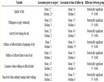
Table 1. Optimised parameters of PECVD grown SiNx and SiOx for encapsulation.
We have used the optimized deposition parameters for inorganic layers for our encapsulating experiments. We first studied the films of alternate layers of inorganic compounds and its encapsulating properties. Encapsulating calcium test lines are show in Figure 1. The approach used is described in Figure 2.
The barrier properties were evaluated for up to five dyads. Then an organic layer (acrylic resin) after two dyads was introduced. This approach is shown in Figure 3. The method used for depositing the same was spray technique, done manually (~1 μm thickness). Two more structures were fabricated using the stack of Figure 3 to evaluate the effective encapsulating property of dyad and organic layer.
3. Results and Discussion
Table 2 summarizes all the encapsulating structures fabricated and their water permeability in this work.
The glass encapsulation was the gold standard for this study. Our goal was to develop a thin film encapsulation at 120˚C that is as good as glass encapsulation.
From one dyad deposited at 120˚C, we observed that it is not adequate barrier


Figure 1. Encapsulation experiments of calcium test lines (black).

Figure 2. Schematic of the inorganic dyad encapsulation of Ca test structure.

Figure 3. Schematic of the two inorganic dyads/acrylic encapsulation of Ca test structure.
Table 2. Summary of the encapsulating structures fabricated and their water permeability.
for water permeability. For a lower deposition temperature we encountered many defects and pinholes in the film, because higher temperature was required for a defect and free film. This is the reason for poor WVTR for a single dyad.
SEM images of the SiOx and SiNx layers were also taken to study surface morphologies. The same are shown in Figure 4. The SiOx film is rougher than SiNx, which was confirmed by profilometer. The defects density is also higher in SiOx than SiNx [22] . Hence, due to these reasons SiNx was deposited over SiOx for smoother encapsulating film geometry (shown in Figure 4(c)). Also, the dyad of inorganic layer was chosen to increase the defects decoupling, and enhancing encapsulating properties of the films.
To overcome the effects on encapsulating behavior due to defect density we deposited another dyad. This makes the path tortuous for the water molecules, WVTR for two dyads in ~ 10−2 g/m2 day. However, adding additional dyads (up to five) only marginally improved the WVTR which can be confirmed by defect densities (cracks and pinholes) present on surface (Figure 4(c)).
In the next structure, instead of adding more dyads, we introduced an organic layer, acrylic resin, deposited using spray technique and cured at 70˚C, on two dyad structure (shown in Figure 3). It reduced WVTR of the two dyad structures almost by two orders of magnitude. This result brought out the important role organic layer plays in barrier film. It filled in the defects present on the top of inorganic films. Figure 5 shows the schematic how organic layer provided additional barrier property by blocking the defects in inorganic layers.
In literature, organic layer has also been used to provide additional tortuous path in the structure. In order to test that, we first added another inorganic dyad on top of the structure of Figure 2. From Table 2, it is observed this does not improve the WVTR significantly. This indicates high density of defects and pin holes. However, adding another organic layer with inorganic dyad on top of this structure (two dyads/organic layer/one dyad/organic layer) exhibits WVTR (~10−5 g/m2 day). As shown in Figure 6, sandwiched organic layer between two
 (a)
(a)
 (b)
(b)
 (c)
(c)
Figure 4. SEM images of (a)SiOx; (b) SiNx and (c) SiNx over SiOx.

Figure 5. Filling of defects of inorganic layer using organic layer.
dyads provides a more tortuous path for the water molecules.
In summary, we have shown an encapsulation scheme at low temperature in which defective structure of the inorganic layers is successfully managed by using two organic layers. The organic layer plays two roles―blocking the pinholes and defects on the surface and second to increase the tortuous path for water molecule in the encapsulation.
4. Effect of Dyads on Flexibility of Devices
As we move on to flexible substrates, flexibility of the encapsulation film also

Figure 6. Tortuous path made by organic layer between two inorganic layers.
plays a vital role. Here we have developed an encapsulating layer with the focus on application to flexible devices. The thickness of each Silicon Nitride film is 400 nm and Silicon Oxide is 300 nm. The organic film (with ~1 μm thickness) adds mechanical strength and flexibility to the overall encapsulating structure. It prevents the delamination due to mechanical strains and abrasion from external sources of the inorganic layers. Hence, providing organic layers between the inorganic ones is beneficial. As the number of inorganic dyads is increased, overall thickness increases and hence the flexibility decreases. But the addition of organic layers provides more flexibility to inorganic encapsulation layer compared to the scene when it would have been absent.
Therefore, in overall terms we can state that although the flexibility decreases as the thickness of the encapsulating layer increases, presence of organic layer in between acts as strengthening factor in flexibility and enhances the flexibility. On the other hand, the overall flexibility obviously decreases with increasing number of dyads.
5. Conclusion and Future Works
In this study we were able to fabricate an encapsulating structure at low temperature capable of providing a barrier for organic solar cells (WVTR~ 10−5 g/m2 day). Even though inorganic layers were very defective, a combination of inorganic dyads with couple of organic layers (sprayed manually) provides WVTR close to that of glass. Further, the experiments of spraying organic layer were not performed under inert atmosphere. Hence, the WVTR value achieved by the proposed structure may turn out to be even better if organic layer is deposited in a glove box or inert atmosphere. The future works include optimization based on thickness of the organic films and further improvement in the defect structure of inorganic layers.
Acknowledgements
The work has been done in complete guidance of Professor Monica Katiyar, Department of Materials Science and Engineering, IIT Kanpur. It has been fully funded by National Centre for Flexible Electronics, IIT Kanpur. The author thanks Samtel Centre, IIT Kanpur for its valuable technical support and advice.
Declaration of Interest
The authors and National Center for Flexible electronics, IIT Kanpur does not report any declaration of interests.
Cite this paper
Kumar, S. and Katiyar, M. (2017) Thin Film Encapsulation at Low Temperature Using Combination of Inorganic Dyad Layers and Spray Coated Organic Layer. Journal of Encapsulation and Adsorption Sciences, 7, 140-148. https://doi.org/10.4236/jeas.2017.74011
References
- 1. Weaver, M., Michalski, L., Rajan, K., Rothman, M. and Silvernail, J. (2002) Organic Light-Emitting Devices with Extended Operating Lifetimes. Applied Physics Letter, 81, 2929-2931. https://doi.org/10.1063/1.1514831
- 2. Reese, M., Dameron, A. and Kempe, M. (2011) Quantitative Calcium Resistivity Based Method for Accurate and Scalable Water Vapor. Review of Scientific Instruments, 82, 085101_1-085101_10.
- 3. Park, J. Chae, H. Chung H. and Lee, S. (2011) Thin Film Encapsulation for Flexible AM-OLED: A Review. Semiconductor Science and Technology, 26, No. 034001.
- 4. Li, H., Liu, Y.-F., Duan, Y., Yang, Y.-Q. and Lu, Y.-N. (2015) Method for Aluminum Oxide Thin Films Prepared through Low Temperature Atomic Layer Deposition for Encapsulating Organic Electroluminescent Devices. Materials, 8, 600-610. https://doi.org/10.3390/ma8020600
- 5. Ahmad, J., Bazak, K., Anderson, L., White, R. and Jacob, M. (2013) Materials and Methods for Encapsulation of OPV: A Review. Review Sustainable Energy, 27, No. 104.
- 6. Dameron, A., Davidson, S., Burton, B., Carcia, P., Mclean, S. and George, S. (2008) Gas Diffusion Barrier on Polymers Using Multilayer Fabricated by Al2O3 and Rapid SiO2 ALD. Journal of Physical Chemistry C, 112, No. 4573.
- 7. Huang, W., Wang, X., Sheng, M., Xu, L. and Stubhan, F. (2003) Low Temperature PECVD SiNx Films Applied in OLED Packaging. Materials Science and Engineering, B98, 248-254. https://doi.org/10.1016/S0921-5107(03)00045-X
- 8. Chen, T., Wuu, D., Wu, C., Chiang, C., Chen, Y. and Horng, R. (2006) High-Performance Transparent Barrier Films of SiOx and SiNx Stacks on Flexible Polymer Substrates. Journal of the Electrochemical Society, 153, No. F244.
- 9. Dennler, G., Lungenschmied, C., Neugebaer, H., Sariciftci, N. and Laterehe, M. (2006) A New Encapsulation Solution for Flexible Organic Solar Cells. Thin Solid Films, 349, 511-512. https://doi.org/10.1016/j.tsf.2005.12.091
- 10. Duan, Y., Sun, F., Yang, Y., Chen, P., Yang, D., Duan, Y. and Wang, X. (2014) Thin-Film Barrier Performance of Zirconium Oxide Using the Low-Temperature Atomic Layer Deposition Method. ACS Applied Materials & Interfaces, 6, 3799-3804. https://doi.org/10.1021/am500288q
- 11. Zhang, S., Xue, W. and Yu, Z. (2015) Moisture Barrier Evaluation of SiOx/SiNx Stacks on Polyimide Substrates. Thin Solid Films, 580, 101-105. https://doi.org/10.1016/j.tsf.2015.02.023
- 12. Martin, Y. (2008) Ultra-High Barrier Plastic. http://people.ccmr.cornell.edu/~cober/MSE5420/page2/files/barrier%20technology.pdf
- 13. Chwang, A., Rothman, M., Mao, S., Hewitt, R. and Weaver, M. (2003) Thin Film Encapsulated Flexible Organic Electronumiscent Displays. Applied Physics Letters, 83, 413-415.
- 14. Gottschalch, V., Schmidt, R., Rheinlander, B., Pudis, D., Hardt, S., Kvietkova, J. and Wagner, G. (2002) Plasma Enhanced Chemical Vapor Deposition of SiOx/SiNx Bragg Reflectors. Thin Solid Films, 416, 224-232.
- 15. Jerman, M., Qiao, Z. and Mergel, D. (2005) Refractive Index of Thin Films of SiO2, ZrO2, and HfO2 as a Function of the Films’ Mass Density. Applied Optics, 44, 3006-3012. https://doi.org/10.1364/AO.44.003006
- 16. Ranade, A., D’souza, N., Wallace, R. and Gnade, B. (2011) High Sensitivity Gas Permeability Measurement for Thin Plastic Films. Review of Scientific Instruments, 76, Article ID: 013902.
- 17. Brewer, P., Goody, B., Kumar, Y. and Milton, M. (2012) Accurate Measurements of Water Vapor Transmission through High Performance Barrier Layers. Review of Scientific Instruments, 83, Article ID: 075118.
- 18. Kumar, R., Auch, M., Ou, E., Ewald, G. and Jin, C. (2002) Low Moisture Permeation Measurement through Polymer Substrates for OLEDs. Thin Solid Films, 417, 120.
- 19. Carcia, P., Mclean, R., Reily, M., Groner, M. and George, S. (2006) Ca Test of Al2O3 Gas Diffusion Barriers Grown by Atomic Layer Deposition on Polymers. Applied Physics Letters, 89, Article ID: 031915.
- 20. Paetzold, R., Winnacker, A., Henseler, D., Cesari, K. and Heuser, K. (2003) Permeation Rate Measurements by Electrical Analysis of Calcium Corrosion. Review of Scientific Instruments, 74, 5147. https://doi.org/10.1063/1.1626015
- 21. Cros, C., Firon, M., Lenfant, S., Trouslard, P. and Beck, L. (2006) Study of Thin Calcium Electrode Degradation by Ion Beam Analysis. Nuclear Instruments and Methods in Physics Research, 257, B251.
- 22. Sobrinho, S., Czeremuszkin, G., Latrache, M. and Wertheimer, R.M. (2000) Defect-Permeation Correlation for Ultrathin Transparent Barrier Coatings on Polymers. Journal of Vacuum Science & Technology A, 18, 149. https://doi.org/10.1116/1.582156