Journal of Modern Physics
Vol.4 No.12C(2013), Article ID:41158,6 pages DOI:10.4236/jmp.2013.412A3001
Synthesis and Characterization of Metal Organic Chemical Vapour Deposited Copper Titanium Oxide (Cu-Ti-O) Thin Films from Single Solid Source Precursor
1Department of Physics, Obafemi Awolowo University, Ile-Ife, Nigeria
2Centre for Energy Research and Development, Obafemi Awolowo University, Ile-Ife, Nigeria
Email: eajayi@oauife.edu.ng
Copyright © 2013 Oladepo Fasakin et al. This is an open access article distributed under the Creative Commons Attribution License, which permits unrestricted use, distribution, and reproduction in any medium, provided the original work is properly cited.
Received September 6, 2013; revised October 7, 2013; accepted November 3, 2013
Keywords: Thin Film; Copper Titanium Oxide; Metalorganic Chemical Vapour Deposition (MOCVD)
ABSTRACT
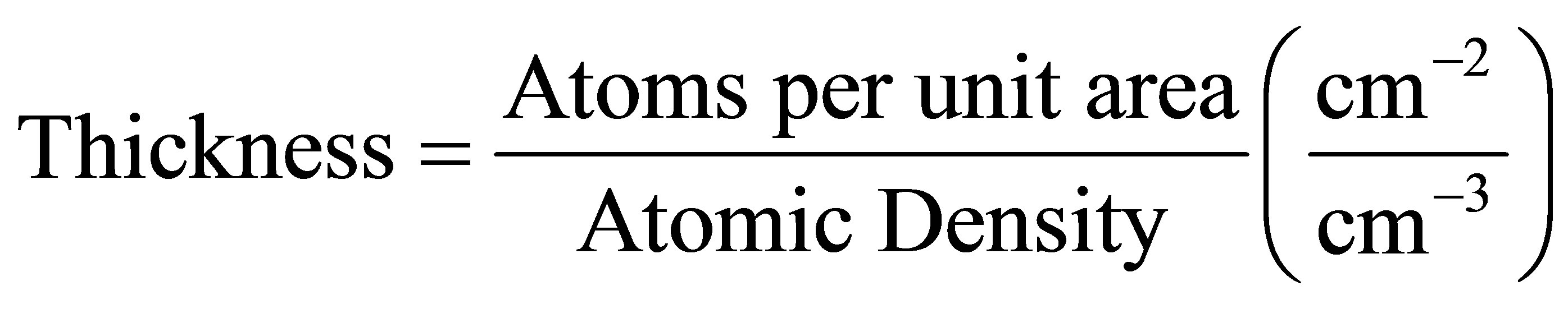
Thin films of copper titanium oxide were deposited by metal organic chemical vapour deposition technique from the synthesized single solid source precursor, copper titanium acetylacatonate Cu [Ti(C5H7O2)3] at the deposition temperature of 420˚C. The deposited films were characterized using Rutherford Backscattering Spectroscopy, Scanning Electron Microscopy with Energy Dispersive X-Ray facility attached to it, X-Ray Diffractometry, UV-Visible Spectrometry and van-der Pauw Conductivity measurement. Results show that the thickness of the prepared film is determined as 101.236 nm and the film is amorphous in structure, having average grain size of approximately 1 µm. The optical behaviour showed that the absorption edge of the film was at 918 nm near infrared with corresponding direct energy band gap of 1.35 eV. The electrical characterization of the film gave the values of resistivity, sheet resistance and conductivity of the film as 3.43 × 10⁻¹ Ω-cm, 3.39 × 10⁶ Ω/square and 2.91 (Ω-cm)−1 respectively.
1. Introduction
Many theoretical and experimental investigations have been carried out on Cu-Ti-O thin film using different deposition techniques in the past. Ideally, the purpose of doping Copper and Titanium oxide is to inhibit recombination of photogenerated electrons and holes by increasing the charge separation and therefore to enhance the efficiency of the photocatalytic process [1]. Cu-Ti-O catalysts are active in deep oxidation of CO and hydrocarbons and selective catalytic reduction (SCR) of NO. The prospects of the application of these catalysts for complex purification of flue gases from NO, CO and harmful organic compounds have been well treated in the literature [2]. Compact Cu-Ti-O thin films deposited on conducting glass are used in new types of solar cells: liquid and solid dye-sensitized photo electrochemical solar cells [3], as well as in solar cells with extremely thin organic or inorganic absorbers [4]. These thin films are also of interest for application in the photo-oxidation of water, photocatalysis, electrochromic devices, among other uses.
In this work, two transition elements (copper and titanium) were considered and deposited as metal oxide thin film. Cu-Ti-O is a mixture of CuO and TiO2 thin films at temperature below 1080˚C which is similar to the phase diagram of Cu-Zr-O [5]. Copper forms two well-known oxides: Tenorite (CuO) and Cuprite (Cu2O). Both the tenorite and cuprite are p-type semiconductors having energy band gap between 1.21 - 1.51 eV and 2.10 - 2.60 eV respectively [6,7]. CuO is attractive as a selective solar absorber since it has high solar absorbency and Cu2O is also a very promising candidate for solar cell application as it is a suitable material for photovoltaic energy conversion [8]. TiO2 thin film has been receiving a lot of attention in the past as the chemical stability, high refractive index and high dielectric constant allow its use as components in optoelectronics devices and sensors [9-11]. The physical, optical, electrical and chemical properties of TiO2 depend greatly on the amorphous or crystalline phase of the material. There are three types of TiO2 crystalline structures: anatase, rutile and brookite. Rutile presents the highest refractive index and is the most thermodynamically stable structure. The anatase structure is obtained at low temperature of around 350˚C, which is useful for industrial applications [12]. At temperatures between 400˚C and 800˚C, the rutile phase is also present, while at higher temperature only the rutile structure is present. Another possible phase known as brookite, but just present at high pressures and high temperatures also exists. Deposition temperatures lower than 300˚C generally result in the formation of amorphous TiO2. It is an n-type semiconductor with energy band gap of 3.2 eV. The change of phase of thin films arises as a result of difference in deposition temperature, thickness and the substrate used [13].When the copper concentration was low, the Cu-doped TiO2 films had the similar anatase phase as the pure TiO2. The sample became amorphous when copper concentration was more than 15.17 at.% and the absorption edge of the sample shifted to longer wavelength region [1].
Most of the studies that have been reported on Cu-Ti-O thin films were of films prepared using complex techniques such as MBE, Sputtering, thermal evaporation, etcwhere multi component precursors were used. In this study the films were prepared by using single solid source precursor, though the technique of using our simple MOCVD set-up has become a standard technique for preparing mixed metal oxide thin film systems.
2. Experimental Method
2.1. Synthesis of Precursor
The single solid source precursor copper titanium acetylacetonate was prepared from acetylacetone, methanol, hydrated copper chloride (CuCl2·2H2O) and titanium trichloride (TiCl3) as chemical reagents. This was carried out by using a modified form of the method reported by Ellern and Ragsdale [14].
8.4936 g of hydrated copper chloride, (CuCl2·2H2O) was dissolved in 60 cm3 of methanol followed by the dropwise addition of 18.5 cm3 titanium trichloride (TiCl3) in 30 cm3 acetylacetone. This was left for several hours and yielded a precipitate of copper titanium acetylacetonate which had a green colour. The precipitate was filtered and left for few days to dry in an oven.

2.2. Film Deposition
Copper titanium oxide thin films were deposited by thermal decomposition of the copper titanium acetylacetonate precursor using metal organic chemical vapour deposition. The apparatus used for the deposition has been reported [15] and the schematic diagram of the experimental set up is shown in Figure 1. The solid precursor Cu [Ti (C5H7O2)3] was ground into fine powder and poured in an unheated receptacle, from where it was blown into the working chamber containing glass substrate holders carrying the substrates. The nitrogen gas was bubbled through at a flow rate of 2.0 dm3/min. The copper titanium acetylacetonate precursor decomposed at the substrate surface in the working chamber which was electrically heated and maintained at a temperature of 420˚C. At this temperature the decomposition of the precursor resulted in the deposition of copper titanium oxide thin films, over a period of two hours. At the end of the two hour deposition period, the gas supply was turned off, and the experimental set up was left to cool before removing the film substrate sample.
2.3. Characterization of Thin Film
The elemental composition and thickness of the film were obtained using Rutherford Backscattering Spectrometry of 1.7 MeV pelletron Accelerator. The structural characterization of the thin films was done using MD-10 model x-ray mini diffractometer with Cu-Kα radiation (λ = 0.15418 nm).The SEM micrographs of the thin films were obtained from a Zeiss DSM 940 scanning electron microscope with EDX detection facility attached. The UV-Visible spectra of the film were run on Jenway UV-Visible spectrophotometer (Model 6405) ranging from 200 to 1100 nm with 5 nm interval. The electrical characterization of the film was done using Kethley Four-point Probe facility (Model 2400) with source voltage of 5 mV.
3. Results and Discussion
3.1. Elemental Composition and Thickness of the Film
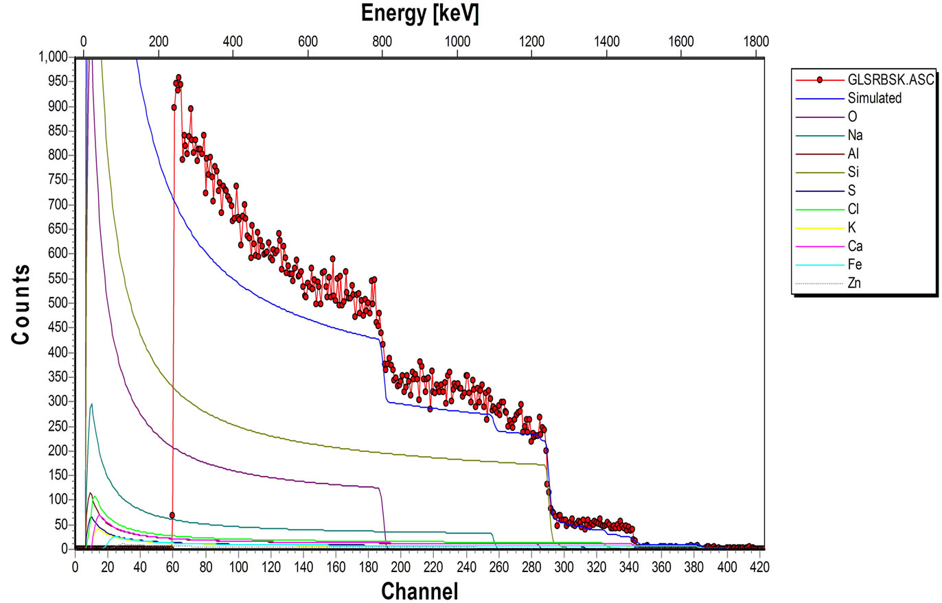
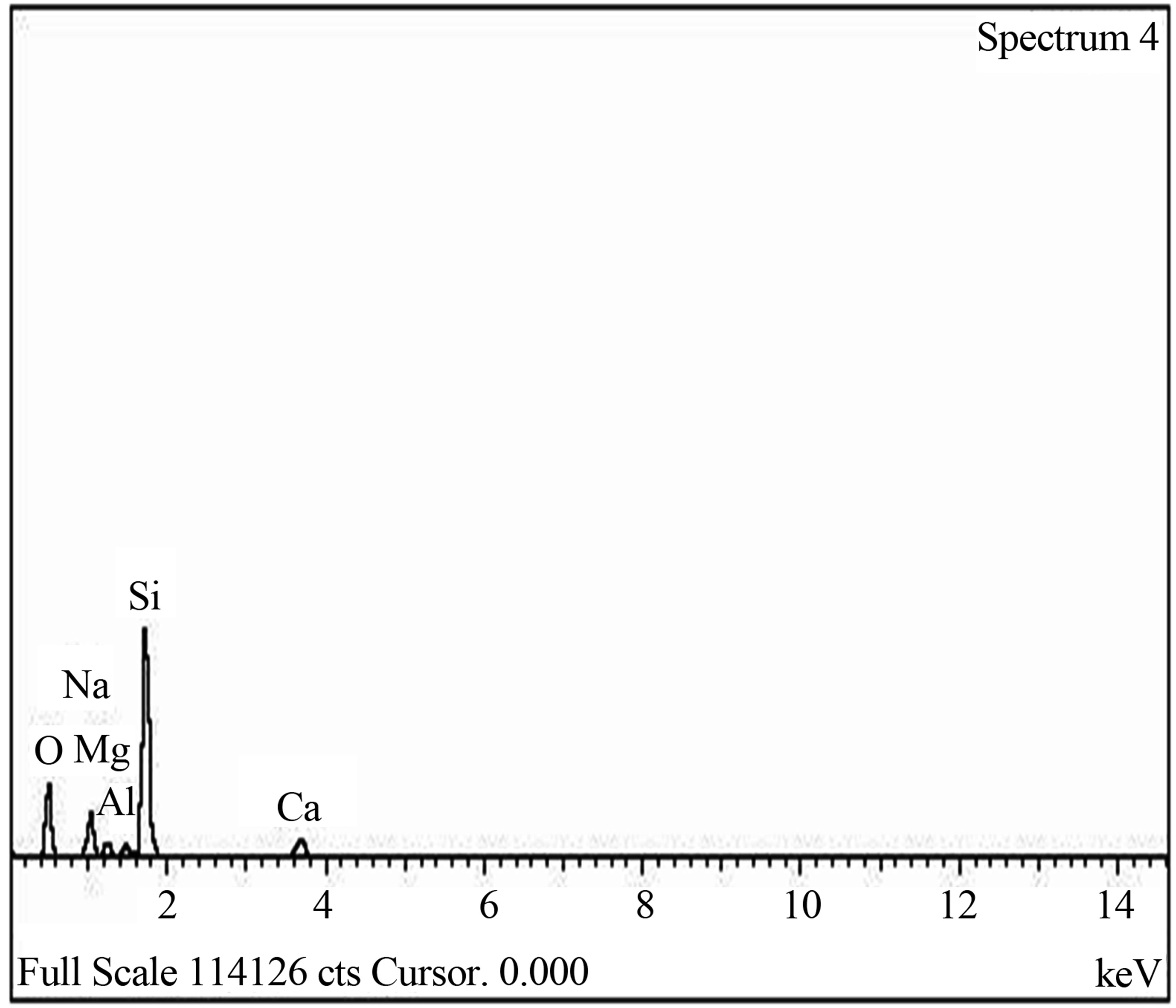
The elemental composition of the soda lime glass substrate was identified using RBS as Na, Al, O, Si, S, Cl, K, Ca, Fe and Zn, (Figure 2(a)). The elements present in the Film/Glass combination are Cu, Ti, O, Na, Al, Si, S, Cl, K, Ca, Fe and Zn (Figure 2(b)). The elemental analysis revealed that the proportions of the film measured are Cu = 51.3736%, Ti = 32.1210% and O = 16.5054% with the film thickness of 101.236 nm using the expression below (according to Chu, et al.) [16].
3.2. X-Ray Study
Figure 3 shows the XRD spectrum of deposited Cu-Ti-O
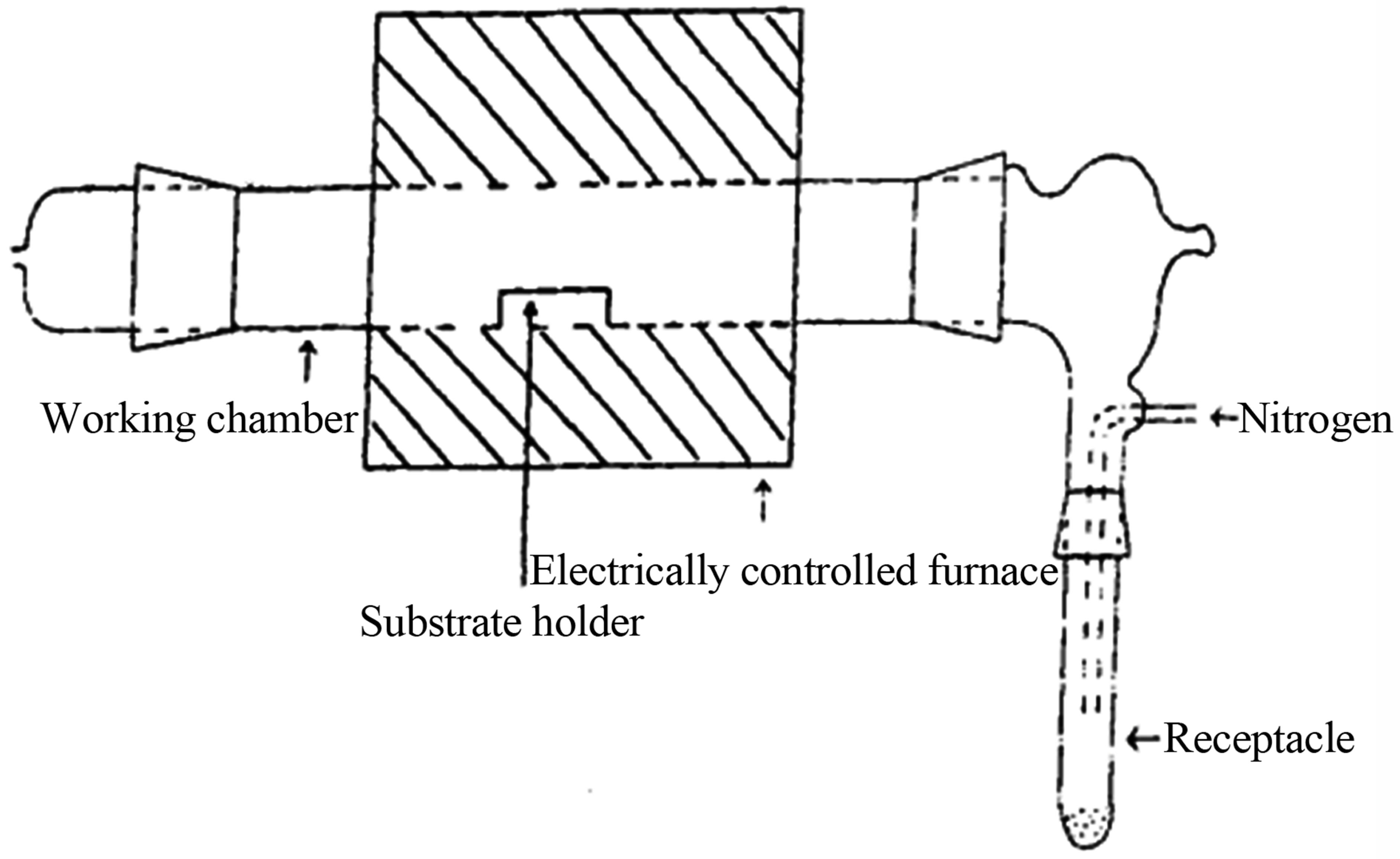
Figure 1. Experimental set up for deposition.
thin film obtained with diffraction angle 2θ ranging from 16˚ to 72˚. There were no peaks that could be used to match the Copper oxide, Titanium oxide or Copper Titanium oxide diffraction data files. Visual examination of the film showed that there was coating on the substrate and the RBS also confirmed the presence of Copper, Titanium and Oxygen in the film. The absence of peaks in the spectrum showed that Bragg’s law of diffraction was not satisfied. The observed featureless spectrum of the film showed that the film is amorphous in structure and thus confirms the glassy nature of the film similar to that reported on cadmium sulfide [17]. This may be due to the fact that the film is porous.
 (a)
(a)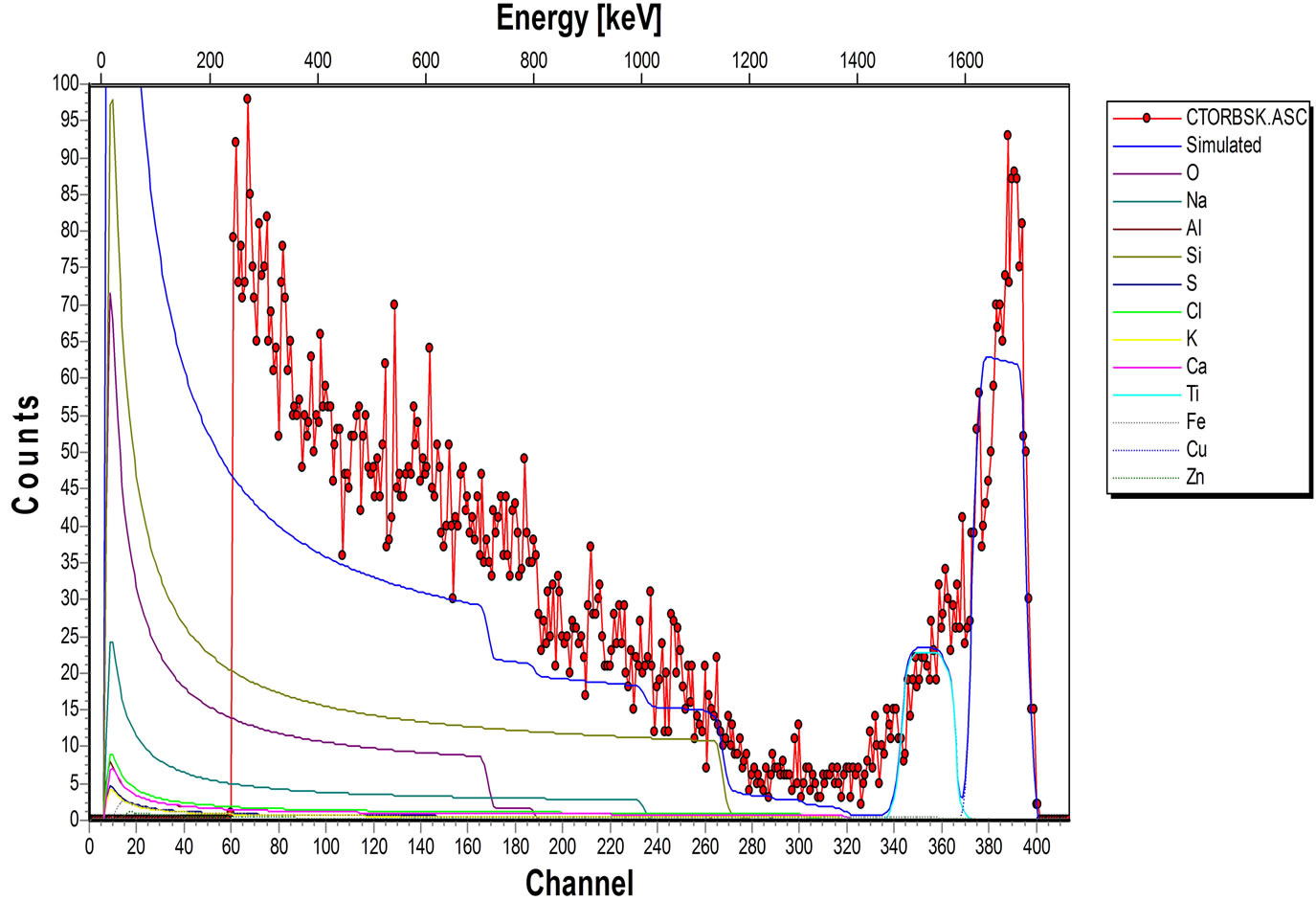 (b)
(b)
Figure 2. (a) RBS spectrum of blank sodalime glass; (b) RBS spectrum of the Cu-Ti-O thin film/sodalime glass.
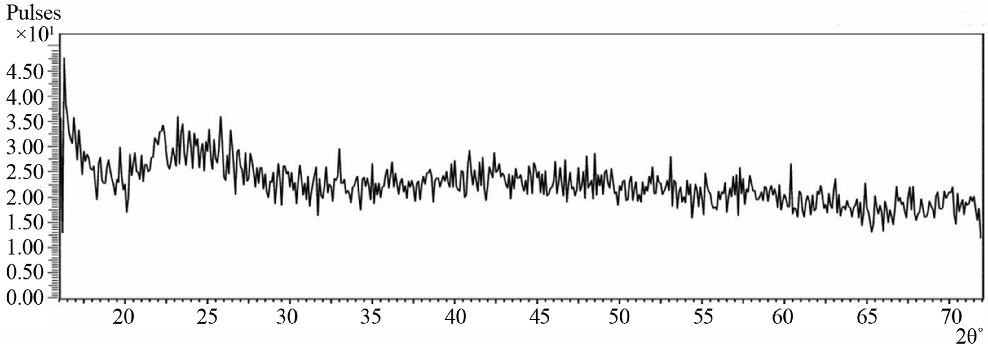
Figure 3. XRD spectrum of the Cu-Ti-O thin film/sodalime glass.
The Bragg’s law of diffraction is given by the expression below
where n is an integer, λ is the wavelength of incident wave, d is the spacing between the planes in the atomic lattice, and θ is the angle between the incident ray and the scattering planes.
3.3. Morphological Study
The SEM micrograph indicated that the film is well and evenly distributed across the substrate surface as clearly shownin the Figure 4. The grains have no regular structure as also confirmed by XRD spectrum and the layers which can be described as overlapping flakes. The average grain size was estimated as 0.924 µm (~1 µm). The EDX spectrum, Figure 5 also confirmed the presence of Copper, Titanium and Oxygen as the elements present in the film.
3.4. Optical Characterization
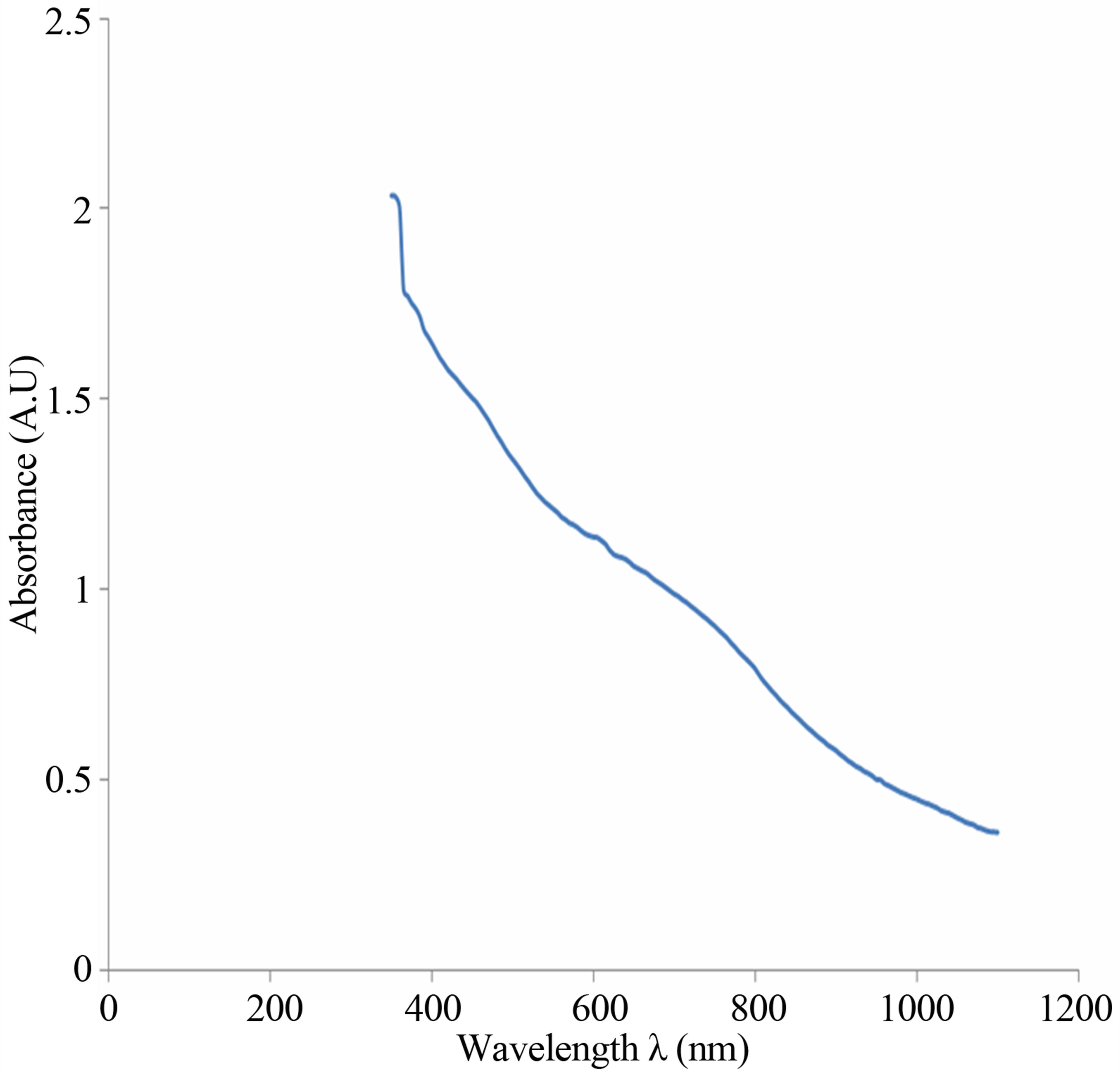
The Ultraviolet-Visible Spectrophotometer gave the absorbance, A of the film as a function of wavelength, λ.
The absorption coefficient is given as
where d, is the thickness of the film measured by RBS.
The energy is given by equation
where h, is the Planck’s constant, c is the velocity of light and λ is the wavelength of the incident beam.
The spectrum of absorbance against wavelength gives the absorption edge as 918 nm (Figure 6(a)). The extrapolation of linear part of absorption coefficient squared (α2) against energy spectrum is 1.35 eV (Figure 6(b)). The absorption coefficient squared against energy confirms that the film exhibits direct band transition. If
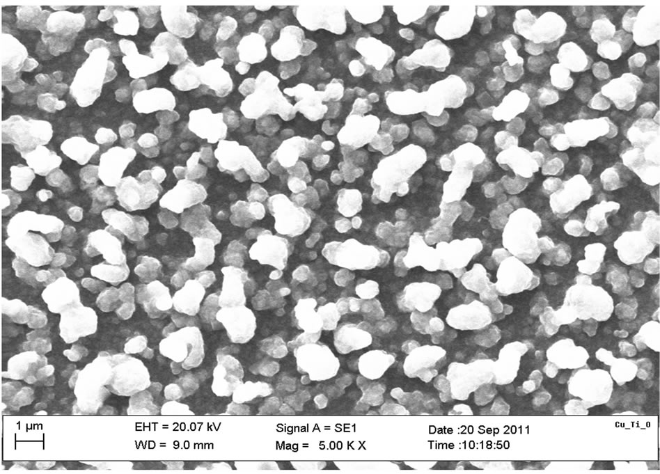
Figure 4. SEM micrograph of Cu-Ti-O thin film.
the Vergad’s rule of mixtures holds for copper oxide and titanium oxide thin film, the result obtained then agrees with the result revealed by the RBS, which gives the percentage of the film as 51.3736% Cu: 32.1210% Ti: 16.5054% O. The film is predominantly more of Copper oxide. The observed increase in the energy band gap of the prepared Cu-Ti-O thin film compared with that of the parent copper oxide is due to the introduction of Titanium into its matrix. The energy band gap of anatase titanium oxide was reported as 3.2 eV [18]. The films which have higher absorption coefficients and direct energy band gap and also meet some other property criteria which may be suitable for photovoltaic applications as absorbing layer, [19] and makes the prepared film suitable for solar cell application.
3.5. Electrical Characterization of the Film
The Resistivity (ρ), Conductivity (σ) and Sheet resistance (Rs) of the film were obtained from the electrical characterization. The average generated voltage and current determined in the study were calculated as 2.92 × 10⁻³ V and 3.90 × 10⁻⁹ A respectively. The resistivity was calculated to be 3.43 × 10⁻¹ Ω-cm, the conductivity was also determined to be 2.91 (Ω-cm)−1 and the sheet resistance
 (a)
(a)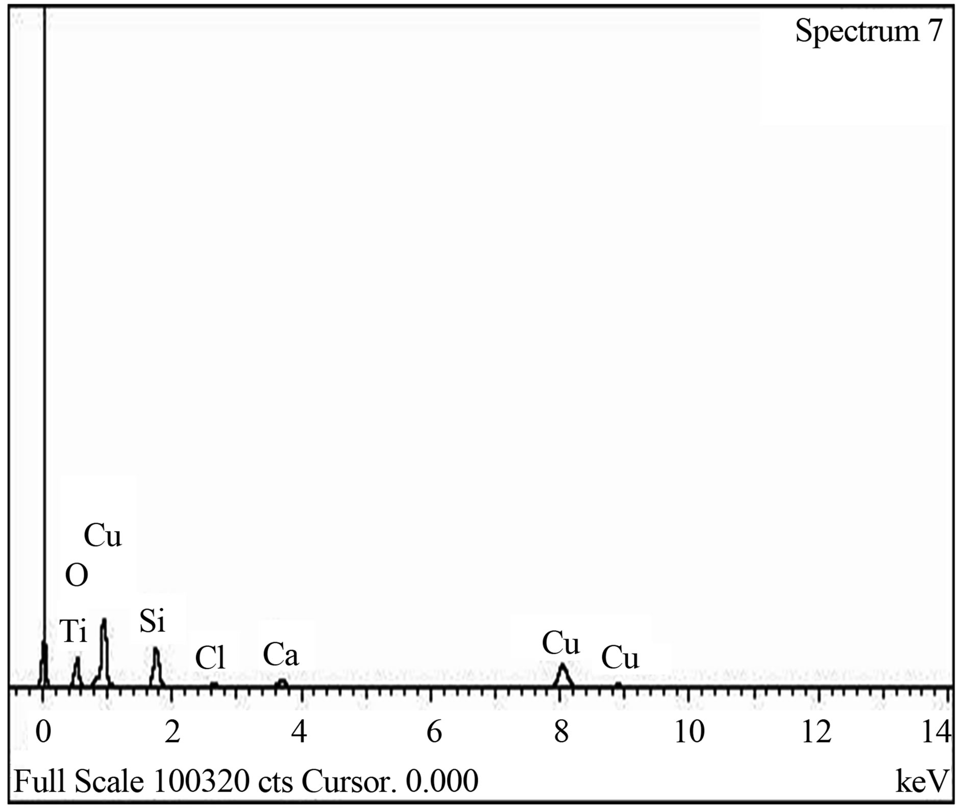 (b)
(b)
Figure 5. (a) EDX spectrum of blank sodalime glass; (b) EDX spectrum of Cu-Ti-O thin film/glass.
of the film was found to be 3.39 × 10⁶ Ω/square. The range of conductivity of copper oxide is as wide as 10−2 to 10−9 (Ω-cm)−1 at very low temperature, depending on the oxygen content of the film [20]. Single crystal titanium dioxide TiO2 has a resistivity of about 1013 Ω-cm at room temperature, and about 107 Ω-cm at 250˚C. At 30˚C, the conductivity is 5 × 10⁻¹⁴ (Ω-cm)−1 but as the temperature is increased to 260˚C, the conductivity increases to 3.3 × 10⁻⁹ (Ω-cm)−1. Therefore, TiO2 is generally considered to be aninsulator at temperatures less than 200˚C [21]. The prepared film is conductive; this was due to the larger percentage of copper oxide present in the films and the deposition temperature.
The resistivity of the film is given as
 (a)
(a)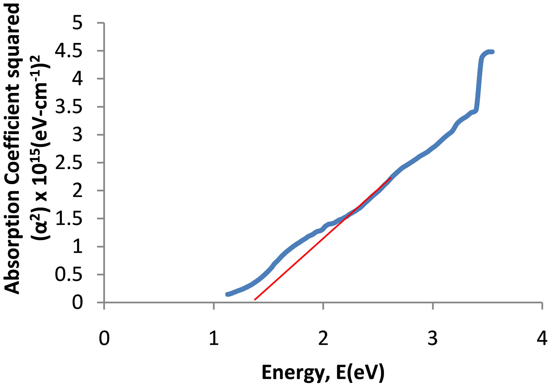 (b)
(b)
Figure 6. (a) UV-visible spectrum of the deposited Cu-Ti-O thin film; (b) The graph of α2 against energy for the CuTi-O thin film.
The electrical conductivity of the films can be obtained by
 .
.
Knowing the values of ρ and thickness of thin films, the sheet resistance can be determined as
 .
.
4. Conclusion
A single solid source precursor of copper titanium acetylacetonate, Cu [Ti (C5H7O2)3] has been synthesized from the metal chloride and solvents using the modified method of Ellern and Ragsdale. The precursor was pyrolysed to produce copper titanium oxide thin film using MOCVD technique. The average thickness of the film was found to be 101.236 nm. RBS analysis had shown that the film is predominantly copper with the percentage of Cu = 51.3736%, Ti = 32.1210% and O = 16.5054% and EDX confirmed the presence of Copper, Titanium and Oxygen as the elements present in the film. SEM and XRD also revealed that the film is amorphous in structure with the average grain size of about a micrometer. The conductivity measurement using van der Pauw technique was determined as 2.91 (Ω-cm)−1. UV Visible analysis revealed that the films have the absorption edge of 918 nm near infrared with direct optical energy band gap of 1.35 eV, which makes the prepared films suitable for solar cell application.
5. Acknowledgements
The UV-Visible and Electrical Characterization were carried out at Engineering and Material Development Institute, Akure, so we thank the staff of the laboratory. Also, our gratitude goes to Prof. E. I. Obiajunwa of the Centre for Energy Research and Development, Obafemi Awolowo University, Ile-Ife for his assistance on RBS analysis.
REFERENCES
- W. Zhang, Y. Li, S. Zhu and F. Wang, Catalysis Today, 93, 2004, pp. 589-594. http://dx.doi.org/10.1016/j.cattod.2004.06.009
- O. V. Komova, A. V. Simakov, V. A. Rogov, D. I. Kochubei, G. V. Odegova, V. V. Kriventsov, E. A. Paukshtis, V. A. Ushakov, N. N. Sazonova and T. A. Nikoro, Journal of Molecular Catalysis A: Chemical, Vol. 161, 2000, pp. 191-204. http://dx.doi.org/10.1016/S1381-1169(00)00342-3
- B. O’Regan and M. Gratzel, Nature, Vol. 353, 1991, pp. 737-740. http://dx.doi.org/10.1038/353737a0
- K. Tennakone, G. R. R. A. Kumara, A. R. Kumarasinghe, K. G. U. Wijayantha and P. M. Sirimanne, Semiconductor Science and Technology, Vol. 10, 1995, pp. 1689-1693. http://dx.doi.org/10.1088/0268-1242/10/12/020
- A. M. M. Gadalla and J. White, Transition British Ceramics Society, Vol. 65, 1966, p. 388.
- K. H. Yoon, W. J. Choi and D. H. Kang, Thin Solid Films, Vol. 372, 2000, p. 250. http://dx.doi.org/10.1016/S0040-6090(00)01058-0
- A. Y. Oral, E. Mensur, M. H. Aslan and E. Basaran, Materials Chemistry and Physics, Vol. 83, 2004, p. 140. http://dx.doi.org/10.1016/j.matchemphys.2003.09.015
- A. N. Banerjee and K. Chattopadhyay, “Progress in Crystal Growth and Characterization of Material,” Elsevier, Amsterdam, 2005. http://dx.doi.org/10.1016/j.pcrysgrow.2005.10.001
- J. Rancourt, “Optical Thin Films (User’s Handbook),” McGraw-Hill, New York, 1987.
- M. Fleisher and H. Meixner, Sensor Actuators, Vol. B4, 1991, pp. 437-441.
- G. A. Battiston, R. Gerbasi, M. Porchia and A. Morigo, Thin Solid Films, Vol. 239, 1999, p. 186. http://dx.doi.org/10.1016/0040-6090(94)90849-4
- D. Mergel, D. Buschendorf, S. Eggert, R. Grammes and B. Samset, Thin Solid Films, Vol. 371, 2000, pp. 218-224. http://dx.doi.org/10.1016/S0040-6090(00)01015-4
- M. I. B. Bernadi, E. J. H. Lee, P. N. Lisboa, E. R. Leite, E. Longo and J. A. Varela, Materials Research, Vol. 4, 2001, pp. 223-226.
- J. B. Ellern and R. O. Ragsdale, Inorganic Syntheses, Vol. 11, 1968, p. 83.
- E. O. B. Ajayi, “Electrical and Optical Properties of Pyrolytically Deposited Indium Oxide,” M.Sc. Thesis, University of Illinois, Urbana, 1970.
- W. K. Chu, J. W. Mayer and M. A. Nicolet, “Backscattering Spectroscopy,” Academic Press, London, 1978.
- D. Kathirvel, N. Suriyanarayanan, S. Prabahar and S. Srikanth, Journal of Ovonic Research, Vol. 7, 2011, pp. 83- 92.
- I. M. Tinginyanu, O. Lupan, U. V. Ursaki, L. Chow and M. Enachi, “Nanostructures of Metal Oxides, Semiconductor Science & Technology,” Elsevier, Amsterdam, 2011.
- F. Atay, V. Bilgin, I. Akyuz and S. Kose, Journal of Optoelectronics and Advanced Materials, Vol. 9, 2007, pp. 3604-3608.
- V. P. Zhuze and B. V. Kurchartor, Physikalische Zeitschrift der Sowjetunion, Vol. 2, 1932, pp. 453-467.
- S. R. Bryce, “Novel Uses of Titanium Dioxide for Silicon Solar Cells,” Ph.D. Thesis, University of New South Wales, Sydney, 2002.