1. Introduction
With the personal intelligent mobile terminal and related products are used widely, it is more and more convenient for information transmission [1]. At the same time, security of personal privacy and even state secrets has become a public concern in the field of security issues [2] [3]. Therefore, abnormal signal detection becomes an important part of security. General special equipment such as spectrum analyzer and others are large, not portable, and expensive. As a result, a signal detection equipment that is flexible, portable and easy to operate has great application value.
2. System Scheme
The equipment architecture of the system has two parts which connected by WLAN/LAN and USB, that is integrated broadband RF signal processing platform and ordinary intelligent mobile terminal with special APP [4], as shown in Figure 1(a). The integrated broadband RF signal processing platform is described in this scheme and display APP will be discussed in the software design part.
The overall architecture of the platform is shown in Figure 1(b). It mainly includes the following components: built-in antenna and external antenna interface, integrated broadband RF transceiver front end (in addition to broadband RF transceiver chip, low-noise amplifier LNA at the front of the receiving channel, NC attenuator DSA, RF preamplifier and RF amplifier for transmit channel, and T/R switch are included), baseband signal processing FPGA, DDR2 mass storage, ARM master, WLAN and USB communication interface.
![]() (a)
(a) ![]() (b)
(b)
Figure 1. Overall scheme of the system. (a) System com- position. (b) Broadband RF signal processing platform architecture.
As a functional design of targeted applications, the following functions are designed based on the function of general signal detection.
The different frequency band signal processing can be completed. In the monitoring state, high-speed frequency sweep function, signal search in the whole band or the specified frequency band and capture of the carrier frequency of suspicious signal are available [5]. After identifying the carrier frequency, the device can enter the panoramic IF state and complete real-time spectrum analysis on the captured signal, intelligent identification or differential separation through the spectrum characteristics, and alarm for the suspicious signal in time. The suspicious signal data can be store in time and upload to the monitoring management center in receiver [6].
The normal signal is collected as the background in advance and the segmentation alarm threshold is set according to the density and the level of the background signal. The abnormal signal alarm is automatically performed.
In addition to timely warning, suspicious signal secret information transmission link can be cut off in the situation of absence of accurate verification [7].
The whole architecture is flexible and open. Therefore, different scenes and functional requirements can be realized through the development of APP. For example, it is anti-tamper while it is also an effective means of collection on sensitive electronic information [8]. It is also very useful in the field of defense. Therefore expansion areas of application are wider than the scope of this article mentioned.
3. Hardware Platform Design
The broadband RF signal processing platform scheme technology line in this paper is the following: monolithic integrated broadband RF signal processing chip as the core, FPGA and other functional modules circuit as supplement [9]. Monolithic integrated broadband RF signal processing chip is a highly integrated solution which integrates analog filters, frequency mixers, data converters, frequency synthesizer in transmit; receive channels and other functions of the digital domain including programmable gain, DC bias calibration, etc. As the device is optimized by orthogonal error calibration and DC bias calibration, the DC offset and orthogonal error limits of zero-IF architectures are dealt and an external filter is not necessary as a result [10]. As the single-chip solution is used in this design to achieve a direct transition from wideband RF to zero IF IQ and eliminate the development of Intermediate links including frequency conversion, filter, sample and digital up and down frequency, pressure of the subsequent baseband treatment is greatly reduced.
The output of the IQ signal connects to FPGA for baseband signal preprocessing through LVDS high-speed link interface which is provided by the chip. The results are put into the mobile terminal through USB or WLAN/LAN com- munication interface for display and some other application operation, while its controlled operation is completed inversely by the mobile terminal through the communication interface [11]. IQ data can be stored in 2 DDR2 storage particles as data that collected by sensitive signals or the memory of the mobile terminal through the communication interface for later analysis. As data source of RF forwarding interference, the store IQ data can also be transmitted as an interfering signal through the DUC and DAC. IQ data of TX can also be derived from the mobile terminal or other GPP [12]. Each emission channel has two antenna feed paths, one of which is low power channel that is connected to the external transmit receive antenna interface and built-in antenna which is switched by T/R switch. Another is high-power channel that is passed through an amplifier and connected to an external antenna via a dedicated external transmit antenna interface.
Based on above design, a Pocket broadband RF processing hardware platform is completed. The method of RF and high-speed digital mixed-PCB is adopted to design a 10-layer PCB circuit board with ultra-thin module and achieve high density layout routing and low height Installation [13]. As shown in Figure 2.
Module integrated RF 2 × 2 transceiver; the frequency range of 70 MHz - 6 GHz; instantaneous processing bandwidth reached to 50 MHz; receiver sensitivity is −90 dBm; linear transmit power is dual 1 W; baseband IQ processing rate is 200 Mbps; the board data storage capacity is 4 Gb; USB2.0 and WLAN communication interface are available. All above are in high-density package with size of 157 mm × 80 mm × 10 mm as the same size with 6-inch screen mobile phone, as shown in Figure 3.
![]()
Figure 2. Pocket broadband RF processing hardware platform layout and electrical material diagram.
![]()
Figure 3. Pocket broadband RF processing hardware platform.
Intelligent mobile terminal is used as the GPP module of the platform and control center with highly programmability [14]. As shown in Figure 4. As the existing mobile phone operating system and hardware resources become increasingly powerful, it is suitable for data process, display and control as GPP [15]. As openness is available, any brand mobile phones can access (also can be PAD and other mobile devices) by using standard USB interface [16] or WiFi air interface. When two mobile terminals with different functions APP are matched with the same hardware modules, two different systems with different functions are generated, which is foreseeable and fit to the open concept of software radio. Pressure on the equipment is further down as the independent removal of the GPP module [17].
Display and control APP based on Android system is developed, achieving the combination of traditional control mode and touch screen operation using ordinary smart phones [18]. A new idea is presented by the scheme in this paper in instrument design and display mode.
Pocket oriented engineering implementation scheme is adopt. In the Pocket broadband RF processing hardware platform, Sanwhich structure is adopt in physical structure meanwhile the traditional shielding box is replaced by splint electromagnetic shielding components [19], meeting the needs of electromagnetic compatibility, supporting the PCB board rigidities, while the size of the module is greatly reduced as the shield structure constitute the shape of the device [20]. The assembly diagram of Pocket is shown in Figure 5.
Great application potential is in the technical scheme of this paper as it has the characteristics of Pocket.
![]()
Figure 4. Mobile display and control terminal mode.
![]()
Figure 5. Pocket platform assembly structure.
4. Design of Display and Control APP Based on Android System
TCP SOCKET connection is achieved on Android platform in the WIFI LAN environment in this design. Android platform APP that developed by Java language connected to the server that established by platform as CLIENT in this system [21].
First, establish a network environment: the platform is set to Service Socket and listening to the port; mobile terminals which are connected to the platform establish Client Socket by platform IP and listening port number (for example: 4060). The underlying operation is achieved through the Android software programming.
In the Eclipse environment, XML language is used as the tool of software interface layout design and properties definition with operation handle is created by the way of “id”. Java language [22] is used to develop the driver of underlying operation. Message is passed between them via “id”.
The flow chart of software control operation is shown in Figure 6.
The main functions of the mobile client display APP are: frequency panorama display, full band scanning, subband display, zoom in and out, mark, trace display, multipoint marking simultaneously, maximum trace, minimum trace, threshold window lines that can be dragged in time, data preservation and so on.
![]()
Figure 6. Android terminal display and control software flow chart.
4.1. Frequency Panorama Display
The panorama display is shown in Figure 7. Frequency panorama acquisition data using SCPI instruction: TRAC? TRACE1; mobile terminal APP sends SCPI instruction to the broadband RF signal processing platform; the spectrum data group that composed of five hundred amplitude data is returned from broadband RF signal processing platform. APP periodically sends SCPI to the spectrum analyzer module through a timer, and then the spectrum data instruction is received by the way of asynchronous thread.
After receiving the data, it is firstly split. Character variable that are composed of amplitude data are split into 500 double type variables and the five hundred double variables are assigned to a double array for convenience of storage.
The open source library AChart Engine is used automatically to display spectrum curve. The horizontal axis of the curve is sequence of 1 to 500 and the vertical axis is the amplitude value of the spectral frequency point. In the display
process, for loop is used to add 500 amplitudes to the curve of the data table, and then the screen is refreshed at the same time and the curve that displayed on the view is updated. Data is received per second and updated the curve simultaneously.
Some of the routines involved in spectrum refresh in APP include:
1) The timer flow;
2) Asynchronous receive data thread code;
3) Data refresh.
4.2. Frequency Band Setting
The starting frequency, termination frequency, the center frequency is set respectively of 1 MHZ, 100 MHZ, 50 MHZ. In order to control the number of threads, the instruction to set the frequency and the instruction to refresh the spectrum data are sent to the same thread. Parameters are input through a text box EditText in the program, and then the format characters for control instruction are added to constitute SCPI control instructions, and then which is sent to the spectrum module through the Socket to achieve control.
4.3. Scaling of Spectrum
As spectrum amplification and reduction are controlled through the two-point slide, it is easy to observe the waveform and in other occasions, which is the special features of intelligent mobile terminals and not available in general equipment.
Touching and listening module the On Touch Listener is used to control zoom in and zoom out [23]:
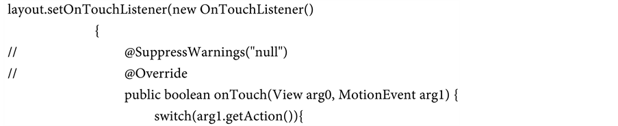
On Touch Listener mainly includes three parts: Motion Event. ACTION_DOWN, Motion Event. ACTION_MOVE, Motion Event. ACTION_UP.
They are respectively corresponding to touching screen by finger, sliding on the screen, leaving the screen. Once action trigger interrupt, coordinates including X and Y value of the contact point are read to achieve action response to the screen.
4.4. Threshold Lines that Can Be Dragged in Real Time
The threshold line window that can be dragged is a function that the conventional signal test instrument does not have, which is an attempt to combine the spectrum analyzer with the Android system. The inspiration comes from Mark and the threshold line, as shown in Figure 8. As threshold line can be dynamically dragged with a certain bandwidth, the peak amplitude value can be measured by dragging. The threshold line that can be dragged uses operation to touch the screen as control interface, capturing the coordinates of the touch point, converting the coordinates to the coordinates of the spectrum display module, comparing the coordinates on amplitude value to calculate amplitude value at the touch point, converting amplitude value at the touch point into a string, us-
ing Text View to display it on the screen, providing feedback control information to achieve human-computer interaction.
As the drag triggering of the threshold line is as the same as the drag triggering of the spectrum view, conflict is presented on the control interface. In order to distinguish them and control respectively, a long press is used to determine the drag object in the program. A long press is achieved by triggering the timer when the screen is touched. If the touch point leaves the screen, the timer event will be clear. If the time to touch screen is so long that the timer value is greater than the set time, the event related to the timer will be triggered and the drag object will be converted to a threshold line.
4.5. Sidebar Slide Menu
In order to use more screens to display spectrum graphics, three ways are used to hide the temporary control in APP.
The first is a pull-up or drop-down control bar. The control group are put in a SCROllVIEW and pulled up or down when they are used, as shown in Figure 9.
The second is alternating display or hiding the next level control bar by clicking the control. The Visibility property of control is set to GONE when they are used or VISIBLE before being used, as shown in Figure 10.
![]() (a)
(a)![]() (b)
(b)
Figure 10. The control bar view to display or hide alternately. (a) The hidden state of the second level control bar. (b) Display status in the second level control bar.
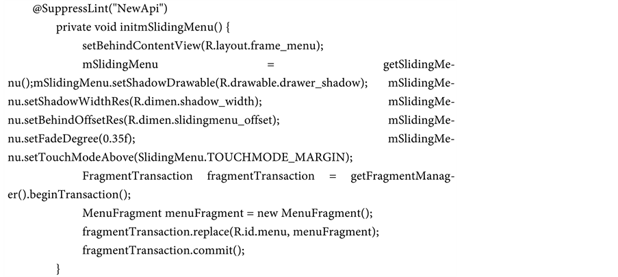
The third is the way of the sidebar to use, that is, the control interface is on the left side of the sidebar and sidebar will be pulled out by sliding on screen from the left edge to the right, as shown in Figure 11. As the addition of Sidebar is relatively complex, open source library Slide Menu is necessary.
The position of the touch point is set to the control interface of the sidebar. The rightward sliding action can be judged when the touch point is in the smaller area on the left and the control sidebar is slid to the right. The initialization code of sidebar is as follows [24]:
5. Summary
The architecture design and hardware platform design of the Software Defined Radio for Pocket is adopted in this paper, realizing a wireless signal detection and control platform with highly integration, simple architecture and small size. Mobile terminal mode that is displayed and controlled by device is proposed and achieved. APP that is used to control and display is developed based on the Andrews system, achieving the combination of the traditional control and display mode and stylish touch screen operation by ordinary smart phones. A new idea is provided in this paper to design new architecture and new control and display mode of instruments.