Atomic-Scale AES-EELS Analysis of Structure-Phase State and Growth Mechanism of Layered Nanostructures ()
Received 25 March 2016; accepted 2 July 2016; published 5 July 2016

1. Introduction
Surface-sensitive methods of electron spectroscopy such as Auger-electron spectroscopy (AES), as well as electron energy-loss spectroscopy (EELS), are widely used to obtain the information not only about the element composition for surface layers (relative quantity of elementary substances) [1] , but also about the change of their structural-phase (the density of valence electrons) and chemical (energy position of electronic bands) states of thin films, as well as about their growth mechanism in the process of film growth [2] . Thus, in general, to obtain this information, values of the energy and intensity of peaks in the EELS and AES, as well as their dependence on the thickness of film are used.
However, traditionally, Auger-spectroscopy finds application primarily in the analysis of bulk samples (see, e.g., reviews [3] - [5] ) and in their profiling by ion etching [6] . In this case, high energy of primary electrons (from 2500 eV and higher) is used for the Auger-analysis. This allows obtaining the better beam focusing and minimizing influence of sample surface onto the results of the analysis of its bulk.
For quantitative Auger-analysis of bulk samples, data on element sensitivity coefficients for almost all substances were tabulated [7] . Often, these data are used for analysis of thin films. Although, in the case of the extremely low thickness of films, using these data is not always justified, it is necessary to determine the element sensitivity coefficients on the experimental data for the given probing depth and other measurement conditions.
In general, the structural and phase analysis of atomic-thin and ultra-thin films has specific character, since it must be done in-situ and under the lowest energy of the primary beam or the lowest probing depth. Moreover, due to the impossibility of the analysis of such films in the air, it is necessary to use all the advanced and extended possibilities of AES and EELS methods.
In fact, there are a number of additional possibilities for the structural and phase analysis of thin films and interfaces, which provide methods of AES and EELS [8] : 1) The dependence of the energy and intensity of the peaks in the EELS on the primary beam energy gives information not only about the thickness of the entire film, but also about the thickness of its layers, and even about the interlayer distance. 2) Analysis of plasma satellite for the substrate Auger-peak can detect the electronic density near the interface layer of the substrate. 3) Quantitative Auger-analysis using a distribution in the attenuation degree as the function of depth allows analyzing the surface structures, which are non-uniform on the thickness. 4) Analysis of the changes in the intensity of the Auger-peak of specific atoms on the substrate surface allows determining the position of the deposited adatoms relatively that of specific substrate atoms.
Typically, in some simple cases (there are no reaction and diffusion between the film and the substrate), using AES and EELS allows determining one of the following mechanisms of the growth: the layered-character growth (LG), island growth (IG), or mixed growth mode (MG) with initially LG and then IG. In more complicated cases (see, e.g., [9] ), the mixing (M) and/or the segregation (S) is necessary to add to these mechanisms of growth: LG + M, LG + S, IG + M, IG + S, MG + M, MG + S. For this purpose, possible not only analyze the thickness dependencies of Auger- or energy-loss electrons of substrate and/or film, but also relation of them, due to the mixing and/or the segregation strongly effect onto this relation. Furthermore, it is possible to analyze the change of atomic density of the film using the energy shift of an energy-loss peak, if the film has a constant element composition on the AES data [10] - [12] .
Joint using of AES and EELS also allows determining the change of structure-phase state of the film/substrate interface in the growth process [13] . This is possible if the probing depth for AES and EELS are identical and cover all the film thickness up to the interface. Initially, the thicknesses of film and attenuation function for film/substrate system are determined by AES analysis. Then, the contribution of the substrate and interface layer in the overall signal is subtracted from EELS by using the attenuation function. After this subtraction and then analysis of energy-loss peak position, the changes in electron density in the film can be detected, as well as interface layer.
It is also possible to determine simultaneously the growth mechanism of film and its thickness based only on data of AES measurements and on known data of probing depth. This can be made by means of choosing one of the possible variants of the growth mode and by means of a procedure of fitting the theoretical curve to experimental points. The following iteration procedure of Auger-analysis can be optimal algorithm of the fitting [9] . At the first iteration step, the film thickness is determined initially under small coatings and for the simplest model of the growth mechanism (usually―the layered-character growth). After that, the model of the growth mechanism is corrected and the thickness is determined under bigger coatings. Then this procedure repeats with correction of the growth mechanism and film thickness at each iteration step.
The purpose of this work is giving an overview of our experience for the analysis of atomic-thin and ultrathin films, to familiarize researchers, who are using AES and EELS analysis methods, with various additional features of these methods and to initiate a wider them use.
2. AES-Analysis of the Composition, Thickness, and the Growth Mechanism
2.1. Quantitative Auger-Analysis of Non-Uniform Nanocoating in Binary System
Auger-analysis of AXB(1−X) (surface coating) − AYB(1−Y) (substrate) binary systems, which are non-uniform on the thickness, is very actual in the study of the initial stages of growth of various hetero-structures and nanocoatings. Examples of such systems are surface silicide phases on silicon [14] . The thickness of the surface phases are usually less than the yield depth of the Auger-electron and significantly lower than the yield depth of backscattered electrons. This allows us to neglect by the contribution of the surface phases in the backscattering factor and simplify the Auger-analysis.
For the quantitative characterization of a AXB(1−X)/AYB(1−Y) hetero-structures it is necessary to determine three parameters: 1) thickness of the coating, 2) composition of the coating and 3) composition of the substrate. But, usually, is known only one of above three parameters and the task is the determining of two others. By measuring two intensities of AES peaks, IS and IV, under two probing depths,  , which are regulating by the AES-peak energy (ES or EV) and primary electron energy (E0), the task can be solved. With this, if the coating thickness (d) satisfies to relations
  and DS > d, then the contribution of the surface coating on the overall backscattering may be omitted and the following system of equations occurs for the ratio of the intensities of the AES-peaks [15] :
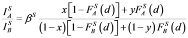 (1)
(1)
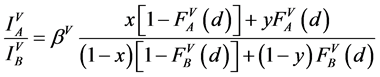 (2)
(2)
 (3)
(3)
where: x, y, z are concentrations of A in the surface coating AXB(1−X), the substrate AYB(1−Y) and a standard sample AZB(1−Z), respectively; F is an attenuation function on the depth [15] , which has form exp(−d/D) for homogeneous system of film/substrate or for a probing depth D identical for the film and the substrate; S is the surface Auger-electrons and V is the bulk Auger-electrons with low (30 - 150 eV) and high (500 - 2000 eV) energies, respectively.
The example of quantitative AES-analysis of the surface coating CrXSi(1−X) on the substrate CrYSi(1−Y) or Si (with homogeneous structure) is presented in the Table 1 [8] , where experimental value of β was used for standard homogeneous sample AZB(1−Z) = CrSi2.
If you connect the composition and the thickness, derived from above AES analysis of corresponding surface phases, with the results of the depth profiling by means of using EELS peak dependence on the primary energy [16] , then you can be possible to form probable structural models of phases presented in Table 1.
2.2. Auger-Analysis of the Adsorption Places on Binary Substrate
Obviously, that the adsorbed atoms C can be arranged with respect to surface A (or B) atoms of binary substrate
![]()
Table 1. Quantitative AES-analysis of thickness and composition in surface phases (on base of [8] ).
AXB(1−X) by various way: I―opposite to A (or B) atoms, II―between A (or B) atoms or III-in random order. Therefore, Auger-peak of A (or B) atoms of the substrate will vanish in varying degrees: I―stronger, II― weaker and III―in moderation. The difference will be more pronounced if A (or B) atoms will be arranged less densely. In this case, we can determine the type of the position of the adsorbed atoms: I, II, or III.
This capability is good demonstrated by Figure 1, in which a dependence on the deposition rate for damping Auger-peak of Cr surface atoms is shown during growth of Si on CrSi2(0001) [17] . For a high surface sensitivity of Auger-peak damping to surface, a lowest-possible energy of the primary beam, 300 eV, was used.
Let us consider the case of the high deposition rate of Si (2 Å/min-curve 1). We can see, that at the first stage, very rapid damping the Cr Auger-peak at Si thickness between 0 and 1/3 ML (0 - 1.17 Å) takes place. This is I-type adsorption, when Si atoms are connected with Cr atoms of the substrate are laying opposite them. At the second stage (between 1/3 ML and 1 ML), damping slows down. This is the adsorption of II-type by means of occupation places between Cr atoms, during which Si wetting monolayer is formed. At the third stage (after1 ML), the Si film grows by the layered growth mode.
In the case of low deposition rate of Si (0.5 Å/min-curve 2), at the first stage (up to 1 ML), the damping slows and there is the adsorption of II-type, when Si atoms are not opposite with Cr atoms of the substrate and are lying mainly between them. At the second stage (between 1 ML and 2 ML), the damping accelerates and the Si wetting layer with the thickness of 2 ML grows by the layered growth mode. And, at the third stage (after 2 ML), the damping slows again and island film is forming without new adsorption places.
Appropriate models shown by the solid line approximately describe stages of growth for both cases. Hereinafter, the models, which are given, use formulas with the damping function for a homogeneous sample in the form of exp (−x/D), where x―the thickness and D―probing depth.
Thus, during increasing the deposition rate, the layered-character growth on the thinner and stable wetting layer transforms to the island growth on a thicker and non-stable wetting layer.
2.3. Quantitative Auger-Analysis of Film Growth Mechanism
Quantitative analysis of Auger-film growth mechanism is facilitated if options for growth mechanisms are given or known. In general, the typical processes of growth are wetting (W), the layered-character growth, LG, and the growth of islands, IG, diffusion-intermixing, M and segregation, S. There are several combinations of these processes for a particular growth mechanism. Figure 2 presents growth mechanisms, when there is a combination of two of these three processes: (a) the layered-character growth, LG; (b) island growth, IG; (c) mixed growth, MG; (d) the layered-character growth with the segregation, LG + S; (e) island growth with the segregation, IG + S; (f) mixed growth with the segregation, MG + S; (g) the layered-character growth with the intermixing, LG + M; (h) island growth with the intermixing, IG + M; (i) mixed growth with the intermixing, MG + M. Other mechanisms of growth are possible, when there is a combination of all three processes of growth (LG, IG, MG) with some combination of W, M and S.
![]()
Figure 1. Auger-analysis of the two cases of the growth of Si on CrSi2 (0001) at a deposition rate of Si: (a) 2 Å/min-curve 1 and (b) 0.5 Å/min-curve 2 [17] .
![]() (a) (b) (c)
(a) (b) (c)![]() (b) (c) (d)
(b) (c) (d)![]() (e) (f) (g)
(e) (f) (g)
Figure 2. Possible mechanisms of growth based on a combination of two from the three growth processes (the layered-character growth, island growth and intermixing).
The objective of quantitative Auger-analysis of the film growth mechanism is a consistent choice of growth mechanisms (according to the principle: from simple to complex), construction of models of the dependence of Auger-signal from the thickness, fitting these models to the experimental data, and choose of the model that provides the best fitting to the experimental data.
The mathematical description of the models may be different in principle. A simple variant of the description is given by the following formula:
1) The layered-character growth. ;
; .
.
2) The island growth.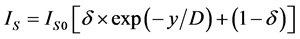 ;
;  (
( ;
;![]() ).
).
3) The mixed growth. I.![]() :
:![]() ;
;![]() . II.
. II.![]() :
: ![]() ;
; ![]() (
(![]() ;
;![]() ).
).
4) The layered-character growth with the segregation.![]() .
. ![]() .
.
5) The layered-character growth with the intermixing.![]() .
. ![]()
where x―thickness of film or deposited material, D―probing depth for AES, IS and IS0 are signals from the substrate with the film and without it, the IF and IF0 are signals from the film and a massive (bulk) sample of the film material, δ is a portion of the surface occupied by islands, y is a effective thickness of the island, kΔ is coefficient of island shape, GΔ is a density of island nuclei, of q is a thickness of the segregated layer and m is a portion of the film material in a mixture (compound).
However, to choose one of three options for growth, it is necessary to build all of these growth models and choose the model that best describes not only the damping of the substrate Auger-signal, but also the film Auger-signal growth. At the same time, this simulation will allow to describe growth and determine quantitatively the composition of the growing layers.
Figure 3(c) and Figure 3(d) show by the solid curves the following different growth stages (I, II, III) corresponding to the fitted models of growth. 1) Stage I is the Fe-Si solid solution formation by diffusion of ~1.5 ML of Si from the substrate (Figure 3(c)) or by FeSi silicide formation (Figure 3(d)). 2) Stage II is the growth of Fe film with segregated Si, which have the thickness of 0.45 ML (Figure 3(c)) or is the growth of Fe3Si silicide formed by intermixing Fe film with 3 ML of Si (Figure 3(d)). 3) And stage III is the Fe layered-character growth (Figure 2(c)). Thus, this simulation allows us to describe quantitatively the growth, the composition and thickness of the growing layers.
![]()
Figure 3. Typical thickness dependences of the Auger-peak intensities for the Fe on Si(001)2 × 1 films in the case of lowered (a) (c) and high (b) (d) temperatures of the beam vapor during the growth [9] . Dashed line is a theoretical curve for the layered-character growth and solid lines are theoretical curves for different growth models (see text).
2.4. Iteration Auger-Analysis of Growth
Iteration procedure of Auger-analysis of the growth consists of the several consequent approximations of the thickness and growth mechanism based on the experimental points of AES peak curve (see Figure 4) [9] .
For a determination of the thickness in the first approximation, the first layers of deposited Fe with the thickness in submonolayer range (first experimental points) are used. With this, the probing depth in the range of several monolayers and the assumption about the layered-character growth mechanism (curve 1) are also used. With this, the attenuation function of the Auger-peak is approximating by an exponential function for the layered growth mechanism. Since first layers for first experimental points have a thickness of lesser than 1 ML and significantly lesser then the probing depth (several monolayers), the value of attenuation of the substrate Auger-peak is almost independent on the model type of the film growth.
The thickness in the second approximation (ordinate axis in Figure 4) was produced additionally from next initial layers under supposition about a more real growth mechanism with the more correct approximation. After the second approximation, next thickness and next model of the growth were generated (curves 2, 3, 4 and 5).
After that, in principle, the next stages of the approximation and next models are possible up to the stabilization of the fitted thicknesses and unchanging growth mechanism models.
3. Structure-Phase AES-EELS Analysis
Using the EELS combined with AES under the identical probing depth enables separates phases and determines their atomic density. Strictly speaking, the determination of atomic density is possible for the phases with the identical composition, as the number of electrons participating in covalent bonds is not changed in this case. Therefore, a position of the plasmon loss-peaks in EELS gives the concentration of valence electrons per unit volume and consequently gives atomic density. And, when an element composition on AES data is changed
![]()
Figure 4. Iteration Auger-analysis of Fe growth on Si(001) for two experiments in different growth modes: ▲is lowered and □ is higher temperature of Fe beam vapor [9] .
gradually during the growth process, then a step change in atomic density during the transition between different phases provides a step change in position of a plasmon loss-peak in EELS.
The attenuation of the substrate EELS signal passing through the film can be obtained if the film thickness from AES data is known. This signal can be subtracted from the total EELS signal [13] [18] . In the result, more detail EELS spectrum of the film itself and also a change in the interface layer of the substrate (if any occur) can be seen.
In overall, when forming films, their EELS correlate with the change of the film element composition if the film density changes little (for example, the formation of a multilayer film of different metals having the dense packing). Or they correlate with the change in atomic density, if the element composition changes little (for example, during structural transition). Last behavior of EELS develops effectively during the sharp change of atomic density (e.g. under the transition of the two-dimensional wetting layer of metal on silicon into the bulk metal phase).
Probing depth has of great importance for an atomic scale analysis by AES and EELS. We have determined that optimal probing depth is near 2.5 Å (EP = 300 eV) for combined AES-EELS analysis of atomic thickness films (with the thickness of 1 - 3 ML) and their interfaces [9] - [13] [17] - [20] .
3.1. EELS Analysis of the Phase Transitions during the Interface Formation
As seen from Figures 1-3, sufficiently smooth form of the Auger-curve is typical one for the metal/silicon interface, which forms usually at room temperature. In this case, the EELS analysis of phase transitions in films with step changing the atomic density is possible. Figure 5 illustrate how the shape and position of the loss-peak in EELS depend on the atomic density of metal film on the silicon substrate. Two cases of phases in the films (and accordingly one phase transition) are considered with different atomic density: 1) two-dimensional wetting layer (WL) of metal on silicon and 2) bulk phase (BP) of the metal.
Below, in the Figures 6-11, family of EELS spectra showing the changes in the interfaces during forming Co, Fe and Cr on the Si(111) and Si(001) substrates are presented. On these figures, E1 and E2 are peak positions of the surface and bulk plasmon losses in the wetting layer 2, and EB is position of the peak of bulk plasmon losses in the bulk phase (metal or silicide) 4. In Figure 6, the peak positions of bulk plasmon losses in differential EELS spectra (see below) for different two-dimensional phases are presented during the formation of a wetting layer.
It is seen, that under certain thickness range, in all the Figures 6-11, there is a non-monotonic increase in the position of peak of the surface, E1, and bulk, E2, plasmon energy losses. With this, there is thickness range with
![]()
Figure 5. The structure of the film-substrate interface (left) and the form of loss-peaks in EELS (right). Were 1, 2, 3 and 4 are interface layer in the Si substrate, a two-dimensional wetting layer of metal (with nonuniform and non-bulk density), Si substrate and metal film, respectively. Loss-peaks 3p, 1p, 2p and 4p are owned: the substrate 3, the interface of layer 1, the wetting layer 2 and bulk phase 4. Peaks 2s and 4s are the total peaks including peaks owned layers 1-4. The vertical dashed line 1e and rectangular column 4e denote of the energy position for bulk plasmon loss-peak in the wetting layer 2 and in the bulk phase 4.
![]() (a) (b)
(a) (b)
Figure 6. EELS of Co films on Si(111) during the partially intermixed interface formation: (a) is full spectra [13] and (b) is spectra obtained by subtracting the substrate contribution (see the next section) [13] .
![]() (a) (b)
(a) (b)
Figure 7. EELS of Co film during formation of the Co/Si(111) interface: (a) with intermixing of Co with Si substrate [10] ; (b) without intermixing [21] .
![]() (a) (b)
(a) (b)
Figure 8. EELS of Fe film during formation of the Fe/Si(111) interface: (a) with intermixing of Fe with Si substrate; (b) without intermixing [13] .
![]() (a) (b)
(a) (b)
Figure 9. EELS of Fe film during formation of the Fe/Si(001) interface: (a) with intermixing of Fe with Si substrate; (b) without intermixing [13] .
![]() (a) (b)
(a) (b)
Figure 10. EELS of Cr film during formation of the Cr/Si(111) interface: (a) with intermixing of Cr with Si substrate [22] ; (b) without intermixing [21] .
![]() (a) (b)
(a) (b)
Figure 11. EELS of Fe films during the formation of the Fe(001) interface: (a) after the deposition of Fe [13] ; (b) after deposition and annealing at 250˚C [13] .
stabilization of the surface plasmon peak position E1. This increase shows the transition from the wetting layer 2 to the bulk phase 3 (a massive metal or silicide). And beginning stabilization of surface peak shows beginning the formation of a wetting layer.
This fact is general one for all metal/silicon interfaces and proves that the formation of a wetting layer under non-equilibrium conditions (deposition at the room temperature) in the metal-silicon substrate system is a general law or general regularity for the formation of the metal-silicon interface. At the same time, as shown in Figure 6(b), the formation of the wetting layer itself is a multi-step process and the formation of various surface phases with different densities and compositions is preceded by its formation.
In the general case, the atomic density of the surface phases is becoming close to the silicon substrate density. And the atomic density of the wetting layer is becoming close to the density of one of the bulk silicides existing in the phase diagram of metal-silicon system. After this, a particular silicide formed depending on degree of equilibrium for formation conditions of the wetting layer. When there is not very high substrate temperature, for example, in the case of the solid phase epitaxy of a wetting layer and in the case of surface phases formed prior to its formation [14] (see Figure 12), the ordering of a wetting layer and these phases occur. This ordering improves the epitaxy of bulk silicides from the wetting layer and determines specific orientation of the silicides.
Thus, EELS analysis is very useful in the study of the formation of heterogeneous interfaces and allows us to trace in detail the stages of its formation. Moreover, this analysis allows us to see the behavior of the atomic density, which is very important for determining the conditions and the mechanism of formation of a wetting layer and its transition to the bulk phase.
3.2. EELS Phase Analysis by Subtracting the Contribution from the Substrate
In the previous section we mentioned about the subtraction of the substrate contribution from overall spectra (see Figure 6). Consider this method in more detail. Figure 13 shows EELS of Co and Fe films on Si(111) substrate after this subtraction [13] .
In this procedure, EELS amplitude of the substrate was adjusted to the value of the EELS amplitude of the film-substrate system using the first approximation of contribution of the substrate into the peak of bulk plasmon losses. After that, the substrate contribution was fitted by correcting form of the bulk plasmon peak in EELS. This is a semi-empirical procedure, since precise definition of contribution of the substrate is not possible due to the fact that the atomic and electron densities of the interface layers of the metal and substrate are modified.
As a result of this modification, in the overall EELS, there is a loss-peak of the modified interface substrate layer in addition to other loss-peaks. Since two of three these loss-peaks are not known, it is impossible to divide precisely the film and the substrate loss-peaks. However, as seen in Figure 13, the subtraction procedure with
![]()
Figure 12. EELS of films obtained by solid phase epitaxy in Cr layers deposited on Si(111) [14] . The right side shows a LEED picture of substrate (Si), ordered surface phase (SP) with the structure of (√3 × √3), ordered wetting layer (WL) with a structure (√3 × √3) and the bulk phase (BP) of epitaxial silicide CrSi2. E1 and E2 are the peak positions in the wetting layer for the surface and bulk losses, respectively. EB is peak position of bulk losses in the bulk phases of Cr.
![]() (a) (b)
(a) (b)
Figure 13. EELS with subtracting contributions of the substrate to interfaces: (a) Co/Si(111) and (b) Fe/Si(111) [13] .
fitting the peak form allows you to select intermediate phases during the formation of a wetting layer and define a range of the thickness for their formation. Thus it is seen that the surface phases are formed at submonolayer- thickness coatings into addition to the wetting phase at a single monolayer-thickness. This suggests about their composition, structure and allows construct the corresponding models of these phases.
3.3. EELS Analysis of Multilayer Films during the Growth
As we have said, the correlation of EELS with the change of the element composition takes place during the formation of the multilayer films of the bulk phases of different metals. Figure 14 shows EELS of a multilayer film of Cu/Fe/Co/Cu on a Si(001) during its growth [19] . From these spectra and peak positions of the surface (white circles) and bulk (black circles) plasmon losses the following is clear. During the formation of all layers
![]()
Figure 14. EELS during the growth of Cu/Fe/Co/Cu multilayer film on Si(001) [19] .
of the multilayer film, initially the growth of a wetting layer and, then the growth of the bulk layer are observed. The only exception is the formation of the first layer of Cu. Here, there is only a formation of a non-bulk wetting layer (with composition Cu2Si or Cu3Si by AES data). And, when Co layer formed, a successive formation of silicides with the CoSi and Co2Si compositions takes place after the Cu layer formation, which is confirmed by AES data. All of these changes would be more clearly seen in the case of a higher resolution of EELS peaks, as well as in the case of a subtracting the contribution of previous layers.
4. Auger-Analysis of the State of Interface on Satellite Peaks
Feature of the fine structure of L23VV-Si peak is that it has a satellite plasmon formed by losses of silicon Auger-electron on the bulk plasma oscillations. An analysis of the position of the plasmon satellite peak in the Auger-spectrum of films provides additional features for the analysis of the emerging interface. Figure 15 shows the results of such Auger-analysis during the growth of Cr (Figure 15(a) and Figure 15(b)) [8] [20] and Fe (Figure 15(c) and Figure 15(d)) [9] on silicon substrate.
The satellite of L23VV-Si peak reflects surroundings of the silicon atoms in Cr film, or at the interface. In the case of a Si substrate, the satellite of L23VV-Si peak allows to find the intermixing between the film and the substrate. In addition, this peak allows tracking the changes in structural or chemical state of the film and interface. So at Figure 15, it can be seen that with increasing the thickness of Cr on Si(111)-7 × 7 (Figure 15(b)) and Cr on the reconstructed by Cr surface with structure of 7 × 7 (Figure 15(b)), the energy of the plasmon satellite reaches the bulk Cr position already at the 3 ML. This indicates the absence of silicon in the film, starting from 3 ML. At the same time, according to the Auger-analysis, there is also no Cr film up to 3 ML. Besides, there is an intermediate energy position of the plasmon satellite in Figure 15(b), when the thickness lesser 3 ML. This shows that, interface silicon and metal atoms form a two-dimensional layer of silicide-like chemical bonds between itself.
In Figure 15(c) and Figure 15(d), Auger-spectra of Fe films on Si(001) are shown under the decreased and increased temperatures of the metal beam vapor, respectively. Analysis of the ratio of Auger-peaks of Fe and Si in Figure 15(c) and Figure 15(d) shows that, in the first case, Fe grows without intermixing at the interface, and, in the second, it grows with forming FeSi and then Fe3Si. With this, the decrease of the energy of the satellite
![]()
Figure 15. Plasmon satellite in Auger-spectra for: 1) Cr films on the Si(111) (a) and Cr films on the surface phase of 7 × 7-Cr (b) [20] and 2) Fe films on Si(001) (c) (d) [9] . Were (c) is growth without intermixing and (d) is growth with intermixing.
peak is seen in Figure 15 in the region 80 eV associated with the bulk Si sp-states in Si. This decrease up to 77 eV is due to an increase of Fe atoms number near Si atoms and with pd-hybridization of Si and Fe bonds at Fe/Si(001) interface. This energy shift of 80 eV peak in Figure 15(c) shows that the Fe bulk phase, bordering with the Si substrate, is formed after 5 ML of Fe. From other side, a saving of the peak position at 5 - 12 ML shows that there is a layer of the segregated Si on the surface. Meanwhile, as it seen in Figure 15(d), the energy position of this peak stays initially unchanged and corresponds to the formation of FeSi after 5 - 6 ML. And then the position is changed and corresponds to the formation Fe3Si after 10 ML.
Another Auger-satellite near 75 eV is associated with the bulk plasmon losses of Auger-electrons in the vicinity of 92 eV. Reducing its energy is connected with the formation of the denser bulk phase of Fe (Figure 15(c)), or its silicide (Figure 15(d)). The disappearance of this peak after 5 ML in Figure 15(c), is due to formation of the cluster or fine-grain structure of Fe film. Such film has a non-uniform electron density and respectively small peak amplitude. At the thicknesses of about 5 ML and 14 ML, the energy shift of the plasmon Auger-satellite in Figure 15(d) is close to the energy of the bulk plasmon losses in FeSi (21 eV) and Fe (23 eV), respectively [23] [24] .
5. EELS Depth Profiling
EELS as an analysis method is currently not widely distributed. It is connected with poor knowledge of given type of spectroscopy, the low resolution of the peaks and low suitability for quantitative analysis because of difficult separability of loss peaks. Another less common method is analysis of the dependency of EELS on the energy of primary electrons. The matter is that this EELS (E) method is not only laborious, but still requires study and improvement of equipment, including measurement automation. While it is clear that this dependence reflect not only the diffraction on grating of the planes of the near-surface region, but also the distribution of electrons output from different depths.
This method uses a ratio of intensities of the elastic peaks of the film and the substrate. In the following example, the film is an ordered wetting layer Cr-Si with the structure of √3 × √3 (intensity peaks―IWL) and the substrate is reconstructed surface of 1 × 1-Cr of the Si(111) substrate (peak intensity―I0). Figure 16(a) and Figure 16(b) show dependence of the ratio, IWL/I0, on the probing depth and dependence, EBP(E), of the energy of the bulk plasmon loss-peak on the primary electron energy [16] .
As can be seen from the Figure 16, these relationships allow carry out profiling of the surface of the wetting layer WL over the depth and determine its thickness. This profiling demonstrates that WL has a thickness equivalent thickness of two double monolayers of the lattice Si(111) and three layers of Cr intercalated in the Si lattice. This information allows finding a model of a wetting layer based on the literature data on its composition and structure, and therefore holding a computer calculation of the parameters of this model.
6. Conclusion
Thus, the review of an innovative methodology for the AES-EELS analysis of atomic-thin and ultrathin films with atomic scale interfaces is given. The methodology provides systematic information about structure-phase state of these films and their growth mechanism. Using this methodology, specific nanophase state of a wetting layer was found, which is formed at the initial stage of growth of the metal film on silicon. This state is characterized by the non-bulk atomic density and determines the film growth mechanism depending on the degree of the film-substrate intermixing.
![]() (a) (b)
(a) (b)
Figure 16. The ratio of the intensity of the elastic peak for wetting Cr-Si (WL) layer with the structure of √3 × √3 to the intensity of the elastic peak for the reference sample with the structure Si(111) 1 × 1-Cr (a) and energy of the bulk plasmon losses for this WL (b) depending on the probing depth, D, and the primary electron energy E, respectively [16] .
Acknowledgements
Research supported by Russian Science Foundation and, in part, by the Federal Agency for the scientific organization and the Far Eastern Branch of the Russian Academy of Sciences (Project No. 15-I-4-015). I thank my collaborators for their help in experiments that formed the basis of these investigations, and V.G. Lifshits for comprehensive support and his contribute to the formation of the basic concepts of EELS.