1. Introduction
Silicon, though dominates silicon industry since a long time due to its superior electronic properties but unfortunately till now efficient light-emitting devices have not been achieved owing to its indirect band-gap and poor radiative recombination efficiency [1] . Nowadays, a great deal of interest has arisen in the synthesis and applications of its porous layer due to its luminescent property [2] -[4] and attracted scientists both from fundamental physics point of view as well as its technological applications [5] . Porous silicon because of its unique properties of spatial confinement, dimensionality (large active) and decrease of reflection losses, etc. stimulated many applications in different fields: light emitting diodes, optical sensors, interference filters, wave guides, biomedical applications etc. [6] Lattice expansion and contraction, anisotropy in nano-crystals and high stress in PS/Si interface etc. are the area still open for research. We present here results from XRD analysis and atomic force microscopy.
2. Sample
Chemical etching, with HF-vapors (CHFVE), of phosphorous doped (100)-oriented CZ-grown silicon wafers (one side polished having resistivity 120 Ω-cm) was carried out at STP in a vapor reaction chamber, Figure 1. Vapors rising from the surface of the acid pass through the tube, directly interact with the sample in the reaction chamber, exit through outlet and dissolve in water. Immediately after etching samples were rinse with de-ionized distilled water and exposed to ultraviolet light, etched surface was found emitting red.
To study the surface morphology of the etched and controlled samples, Atomic Force Microscopy (AFM) was carried out under a collaborative arrangement with Institute of Semiconductors, Beijing, China. Structural properties of the samples were also studied using XRD technique. The difference in surface morphology and XRD patterns of etched and un-etched samples was examined and results obtained are presented below.
3. Results and Discussion
Typical XRD pattern of un-etched samples obtained with JDX-3532 using copper kα line of wavelength λ = 1.5418 Å shown in Figure 2(a), Figure 2(b) depicts four intensity peaks at 2θ = 67.5, 69.35, 69.44, 69.64 and 75.63. This pattern was compared with the pattern reported by Jams D Rachwal [8] and Sudesh et al. [7] for (100) silicon single crystal. Jams D Rachwal has shown the scan for XRD reflections from Cu(kα1) and Cu(kα2), Figure 2(c). After correction, Figure 2(c1), for Cu(kα2), only one single peak at 2θ = 69.15 was left reported by other authors also [8] -[11] . The comparison of XRD patterns for our controlled sample {silicon (100 and reported by Jams D. Rachwal (Figure 2(c1)) reveals that intensity peak appearing at 2θ = 75.6 in XRD pattern of controlled samples is not due to Cu(kα2) line but it may be due to the formation of some unknown species like oxides of silicon on the surface. Similarly intensity peak appearing at 2θ = 67.5 is also due to some unknown specie formed on the surface. The small peaks appearing as right and left shoulders may be due to stressed induced planes at the boundaries of the grains.
XRD pattern, Figure 3, for etched samples shows that reflections from (100) planes appear at 2θ = 69.44, the same 2θ values as were noticed for controlled samples. Interestingly reflections at 2θ = 75.6 and 67.5 disappeared after etching which confirms that these reflection has nothing to do with structural properties of silicon. The disappearance of shoulder peaks high lights the removal of stress related planes at the boundaries of the
 (a)
(a) (b)
(b) (c)
(c)
Figure 2. (a), (b): X-ray diffraction patters of the unetched etched sample; (c): c1 before and c2 after stripping Cu[Kα2] off the raw material [8] .
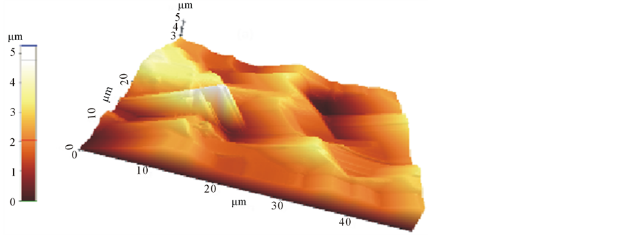
grains. A new intensity peak appears at 2θ = 29.32. This new intensity peak can be assigned to porous layer formed at the surface of (100) silicon. Lower value of 2θ indicates the higher values for inter planer spacing (d values) of atomic layers of porous silicon. The comparison of X-rd pattern with the pattern reported by Aouida et al. [11] for SiOx/Si-containing NH4SiF6 reveals that reflection appearing at 2θ = 29.32 in the pattern for our etched samples is closer to the reported (220) reflection. Three dimensional AFM images, Figure 4, of etched silicon surface high-lights the formation of porous layer on the surface of silicon samples. Pyramids like hillocks with etched channels on the slopes. The base dimensions of pyramids at the base are roughly 1 µm × 1 µm and height 1.5 µm. The dimensions at the top are not clear, however minimum dimension of etched pits are roughly 50 nm. The channel width is roughly 25 nm. Overall pore structure is consisted of more complicated network of etch pits and pyramids. It can be visualized that this porous surface may generates confined emitters of different energies depending on the dimensions of features existing on the surface.
The chemistry that occurs [12] [13] at a silicon surface during vapor etching involves a competition between Si-O, Si-F, and Si-H bond formation. Si-O bonds are chemically attacked by F and significant quantities of Si-O species only form under conditions in which the rate of diffusion of F to the silicon surface takes place. When the concentration of HF vapors is low, oxidized silicon atoms are generated at the surface too rapidly to

Figure 3. Typical x ray diffraction pattern of etched samples.
be attacked by F and water molecules take over the simplified mechanism for etching of Silicon surface (fluoride-containing Si surface). The reaction mechanism shifts to Si-O formation and the reaction stoichiometry transitions from 2-electron to 4-electron. The lack of fluoride ions means that the oxide cannot be removed from the surface; this insulating oxide terminates propagation of the pore. The valence band holes are then required to move into the porous silicon matrix to oxidize a Si atom that is accessible to the fluoride ions instantly formed on the surface. The result is thinning of the pore dimensions close to the porous silicon/crystalline silicon interface. When silicon sample surface is fully covered with HF solution, the oxide dissolves and the surface becomes terminated with H atoms. This is puzzling if one considers that Si-F is the most thermodynamically stable bond in all of silicon chemistry; the relative strength of bonds increases in the order Si-H < Si-O < Si-F. Si-F bonds are highly polarized due to the large electro-negativity of fluorine, and Si-F surface species is much more susceptible to attack by nucleophiles than Si-H species. So in a sense, the Si-F bond is to strong; if a fluoride ion attaches to a silicon atom, that atom is rapidly attacked by additional fluoride ions and removed from the surface. The surface silicon takes two paths, depending on the availability of fluoride ions. Reaction follows a path when excess of HF is present (excessive HF diffusion) on the surface and oxidation of silicon occurs on the surface. Reaction follows the other path if HF diffusion is low, water attacks the surface and an insulating oxide is generated and the silicon atoms capped with H atoms thus predominate on the surface during etch: hydrogen is much less electronegative than fluorine, and a surface with Si-H species is less susceptible to nucleophilic attack. At the end of an HF etch, porous silicon samples contain primarily Si-H, SiH2, and SiH3 surface-groups with minor concentration of O or F related species [14] . Kabbi et al. [6] has shown that Quantum confinement and surface passivation are responsible for the electronic states of the silicon nanocrystallites. A part of porous layer may be related to electron (or even excitons) trapped by Si-O [15] bonds that produce localized levels (energy states) in the band gap of nano-crystallites smaller than few nm.
The comparison of XRD pattern with the pattern reported by Aouida et al. [5] for SiOx/Si-containing NH4SiF6 reveals that reflection appearing at 2θ = 29.32 in the pattern for our etched samples is closer to the reported for (220) reflection. To understand the role of micro features on the surface of porous silicon, the knowledge of their structural and physical properties is essential. AFM is a versatile non destructive technique, capable of probing single micro surfaces at high resolution, in material science to elucidate surface morphology of the material. The technique gives a new insight into the surface morphology by providing three-dimensional images of the surface with molecular resolution, in real time and with minimal sample preparation. AFM images, shown in Figures 4(a)-(c), revealed a number of complex surfaces of different dimensions/structures appearing
 (a)
(a) (b)
(b)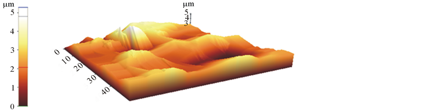 (c)
(c)
Figure 4. AFM image (µm) of etched siliconscan (a) 2D; (b) in X-; (c) Ydirection.
on the etched surface which are of the order of nm. The dimensionality of the structures and number of complex surfaces suggest the generation of a number of irradiative recombination centers responsible for emission of luminescence due to electron confinement may be of different colors depending on the energy states induced by electron confinement in the material having few atomic dimensions. The emission of a single color is due to dominant formation of microstructures having similar dimensions. Our samples are etched with very slow rate of HF vapors that reduces the concentration of fluoride ions to interact with surface, which means minimum removal of oxides from the surface or in other words formation of oxide layer (passivated layer) that may be of the order of Bohr radius. In our opinion red emission is either due to confinement of electrons in nano-crystallites or passivated layer of few atomic dimensions.
Acknowledgements
Atomic force microscopy of the samples was carried out in Institute of Semiconductors, China, under a collaborative program and other measurements were performed (on payment) at CRL, Peshawar University Pakistan. Etching reaction was performed in Science Laboratory of Denial High School, Rawalpindi.