A Novel Adjustable Plasmonic Filter Realization by Split Mode Ring Resonators ()
1. Introduction
Plasmonics and integrated optical devices play an important role in routing, switching and controlling of light in the various fields of modern optical communication and networks [1]. Plasmonic waveguides transfer the electromagnetic waves coupled to surface collective oscillations of free electrons on a metal, called Surface Plasmon Polaritons (SPPs). The SPP waves are bound to and propagate along metal-dielectric-metal interfaces [2]. The light confinement below the diffraction limit is the main identity of plasmonic waveguide making them different from other types of optical waveguides such as photonic crystals, optical fibers, etc. Furthermore, the introduction of deep-submicron technologies in electronic engineering leads to a revolution in optoelectronic circuits [3]. Various structures such as nano-particle plasmon waveguides [4-6], Domino plasmon waveguide [7], grooves and wedges [8-10] and Metal-Insulator-Metal waveguides (MIM) [11,12], are introduced by transporting SPPs. In addition to the fabrication simplicity, high degree of SPP confinement and compact size have made MIM geometry the most attractive among other nanosclae waveguides [13]. Different types of plasmonic filters such as tooth shaped subwavelength, and add-drop topologies are introduced and analyzed by numerical methods such as Finite-Difference Time-Domain (FDTD) [14,15]. It has been shown that the transmission spectra of an asymmetrical multiple teeth-shaped structure can present a narrow band pass filter [16]. Moreover, ring resonator filters generate opposite phase standing waves using optical cavities, to be used as a suppressor of some targeted wavelengths in the transmission spectrum [17]. Depending on the position of cavities relative to the main MIM guiding structure, it is possible to achieve band pass (two MIM waveguides coupled to each other by a circular ring resonator) or band stop filters (laterally coupling ring resonator to an MIM waveguide) [18]. One of the most interesting applications of MIM waveguides that have been the subject of many recent papers is the construction of integrated plasmonic optical filters by cavity waveguide coupling [19,20]. Coupled Mode Theory [21] and numerical methods [22] are used for the analysis of such structures. Optical filters, as one of the building blocks of integrated optical circuits, are recently introduced in different geometries such as bidirectional wave coupler based on Bragg Gratings [21,22], bidirectional splitter in different angles of incident light [23], plasmonic splitter based on the MIM waveguide with periodic grooves [24] and wavelength de-multiplexer based on MIM plasmonic nano-capillary resonators [25]. The introduced structures suffer from some limitations such as huge dimension for splitting functionality [21,22, 24], insulation lack between output ports [23], low transmittance [21-24], power leakage [21-23], and maximum fanout of two for splitter channels [21-24]. An annular ring being able to support multi-modes, should gratify the boundary conditions. Coupling and perturbation methods are used for the resonant mode excitation [23].
In this paper, a novel nanoscale plasmonic filter is introduced while its functionality is verified by numerical simulations in different configurations. Next section describes the dispersion relation for the introduced filter. While the theoretical model is presented in Section 3, Section 4 describes the transmission spectrum results.
2. Dispersion Relation and Effective Refractive Index of MIM Waveguides
Figure 1 shows a MIM waveguide, where each metal/ dielectric interface allows SPPs with a TM mode to propagate along x direction. It is shown that whenever the separating space between two interfaces is comparable to the decay lengths of SPPs in the dielectric region, the SPPs get coupled to each other and confined in the dielectric region between two metals [1]. The field analysis inside the dielectric space between two metals could be achieved using Maxwell’s equations:


in which β is the propagation constant of the MIM waveguide and 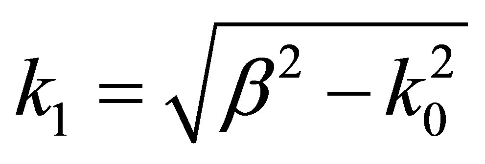 is the wave vector normal to the propagation direction and k0 is the propagation constant of free space. Using boundary conditions and the field components in the metal region, the dispersion relation of MIM waveguide structure could be calculated by:

where indices 1 and 2 denote the dielectric and metal layers, respectively. Silver is regarded as the metal in this paper, and Drude-Lorentz model with five poles is used for dielectric constant determination [25]:
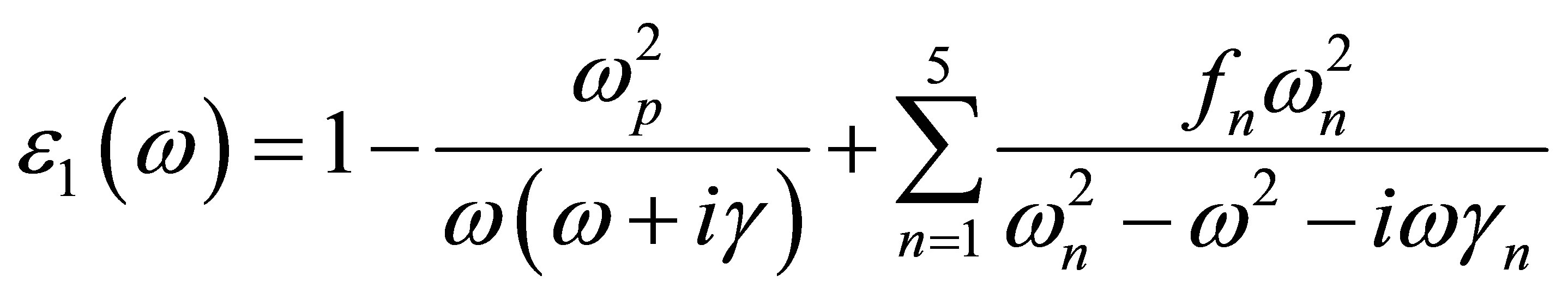
where ωp = 2002.6 THz is the plasma frequency and γ =

Figure 1. Schematic representation of an MIM structure with two semi-infinite metal slabs of permittivity ε2 surrounding a dielectric layer of thickness h and permittivity ε1.
11.6012 THz is the damping constant. Table 1 summarizes the main values for dielectric constant calculation, i.e. ωn resonant frequencies of silver, damping constants γn , and oscillator strength fn [25].
3. Theoretical Model
The Local Split Resonant (LSR) mode of a circular ring resonator and its effects on the transmission spectra is investigated in this paper theoretically and numerically.
Figure 2 presents the LSR mode excitation using different impedances on the ring resonator. The coupling separation distance Δ is 10 nm and the device length l is set to 1 µm.
The input and output MIM waveguides are coupled by means of a LSR ring resonator made out of two sectors with different impedances. Sector (I) with inside and outside radius of a0 and b0, and r0 as the average , has a higher characteristic impedance in compare with sector (II) with inside, outside and average radius as ai, bi and
 , respectively. Solving the wave equation in cylindrical coordinates, field distribution in region (I) can be written as:


where,  for
for , and n is the nth roots of Bessel functions of the ξth order which has infinite discrete roots, and
  and
and . In these equations
  and
and  are the wave numbers in region (I) and region (II), respectively. Furthermore,
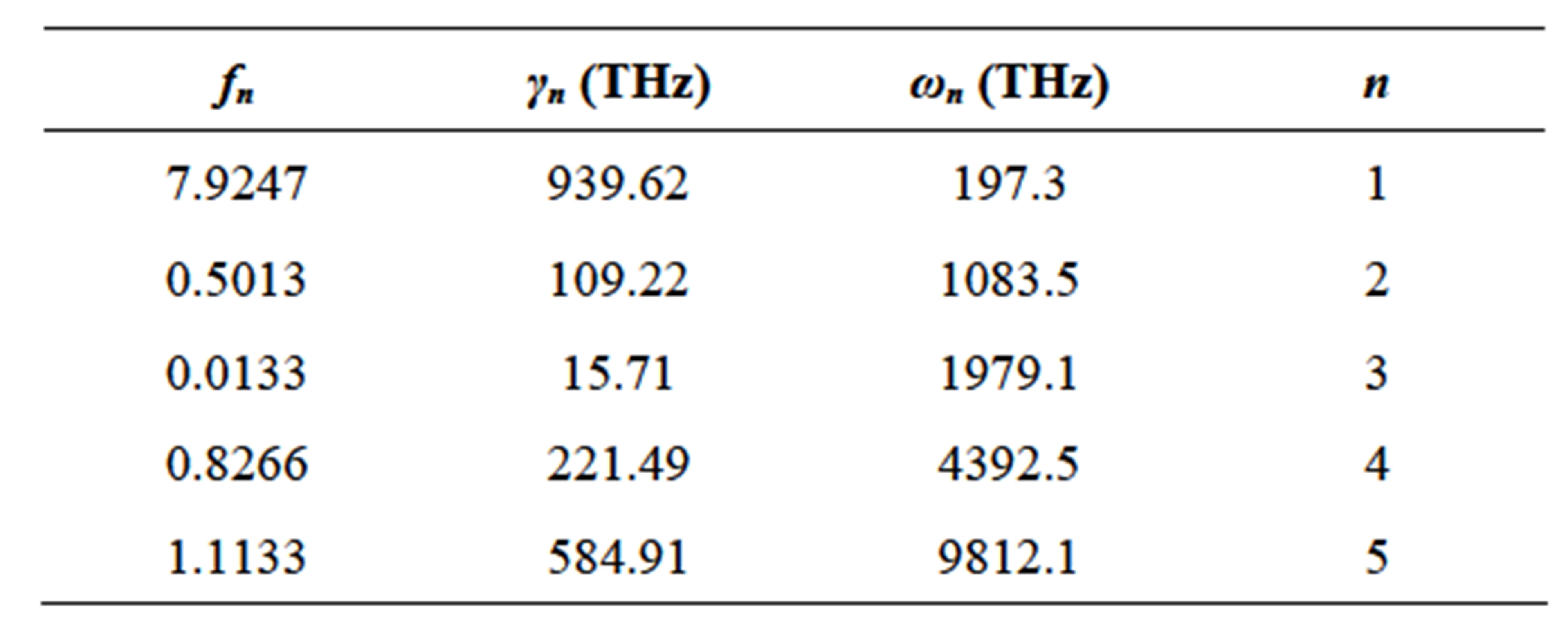
Table 1. Silver values for evaluating Drude-Lorentz model.
 (a)
(a) (b)
(b)
Figure 2. (a) Schematic of the split mode circular ring resonator with an increasing sector between −φ0/2 and φ0/2, (b) Schematic of the split mode circular ring resonator with a decreasing sector between −φ0/2 and φ0/2.
field distribution for region (II) can be calculated from:


where,  for
for ,
,  and m is the mth roots of Bessel functions of the vth order. Jv and Yv represent the first kind and second kind Bessel function of order v, respectively. Using boundary condition at ρ = ai and ρ = bi in region (II), and either one of ρ = a0 or ρ = b0 for region (I), one obtains:


and

In addition, using the continuity of tangential components of the magnetic fields at φ = φ0/2 and φ = -φ0/2, it can be found that


In conclusion, the characteristic equation is obtained being useful for mode calculation in sector (I).
Similarly, characteristic equation for sector (II) can be found as:

It should be noted that n = 0 and m = 0 are not acceptable for all of these equations because of existence of second order Bessel functions in the equations. In fact, each of these sectors follows its individual characteristic equation to illustrate encompass modes in any wavelength. However, instead of using TMv.m and TMξ.n for each sector, it is preferred to use one notation to specify modes of the whole ring structure which is made of two sectors with different radial widths. Hence, in this study  is defined to show the split mode ring resonator in which, the upper index refers to the mode of the manipulated sector, with angular width of φ0, and the lower index refers to the mode of the main shape, with angular width of π - φ0 for
 . Using a unique notation is applicable when both TMv.m and TMξ.n exist. If one of these modes does not exist, we cannot use this notation and it is essential to use another one. For example, in this study, if there is no propagating mode inside region (II) or region (I),
  and
and , are only used respectively. However, it should be noted that, these resonant modes build a local resonance inside the manipulated sectors and other resonant modes which cannot satisfy the local resonant condition, are lost due to scattering inside the manipulated regions. For example, considering φ0 = π/6, it is anticipated that only the ξ = 6p (integer multiples of sixth) mode maintains the resonant condition and other modes split.
4. Plasmonic Filter with a LSR Circular Ring Resonator
4.1. Typical Band-Pass Filter with a Circular Ring Resonator
Figure 3 shows a typical plasmonic band-pass filter by the means of a circular ring resonator consisted of two MIM waveguides coupled together by a circular ring resonator [14]. The main parameters are Δ, a, b, r and h describing the coupling separation and the ring resonator, inside, outside and the average radius of the ring resonator, and the MIM waveguides width, respectively. In this investigation, in order to have fundamental mode (TM0), h is considered to be 50 nm; to achieve a definitive subwavelength structure. In such structures it is essential to monitor the input signal (T1), the output signal (T2), analyzing the power in the frequency domain to reach transmission coefficient, defined as output power divided into input power, T = Pout/Pin. Figure 3 shows the transmission spectrum of a typical circular ring resonator with Δ = 10 nm, a = 100 nm, b = 150 nm as the main property of the filter.
 The filter is placed in a length of L = 1 µm. It can be seen from Figure 3(b) that there exist two resonant peaks, related to two different resonant modes with the wavelengths of λ1 = 1162 nm for the first mode, and λ2 = 602 nm for the second mode. Considering ri and ro as the inside and outside radius of the ring resonator, respectively, it is shown that these modes can be computed using the following equation [23]:

in which  is the wave number,
  , εr and μr are light speed in free space, relative permittivity and permeability, respectively. It can be shown that the effective refraction index of a MIM structure can be computed as [1]:
 (a)
(a) (b)
(b)
Figure 3. (a) Schematic of a typical plasmonic MIM bandpass filter using a circular ring resonator, (b) The transmission spectrum of a typical plasmonic MIM band-pass filter using a circular ring resonator.
The transmission simulation of the filter is calculated using 2D FDTD and is shown in Figure 3(b). In these simulations, it is assumed that the size of each uniform Yee cell of the structure in x and z-directions are Δx = Δz = 2 nm. The computation domain of this structure is a conventional perfectly matched layer (CPML) absorbing boundary condition.
4.2. Adjustable Plasmonic Filter Using a Split Mode Ring Resonator
This section investigates the effect of using a split mode ring resonator on the main modal characteristics. In fact, the split mode resonator is made out of two or more changed impedance circular sectors on the circular ring. Due to impedance changing, a local resonant boundary condition is created which can reserve or split the different mode’s energy. It is assumed for simplicity that the constant coupling distance Δ, was setting as that in the investigated structure (see Figure 2).
In order to study the effect of the position of the manipulated sector on the transmission spectrum of the ring resonator filter, one can observe Figure 4 in which φ0 is
 (a)
(a) (b)
(b) (c)
(c) (d)
(d)
Figure 4. (a) The transmission spectrum of the split mode ring resonator plasmonic filter for even values of m in an decreasing split sector with a0 = 110 nm, b0 = 140nm, constant φ0 = π/3 and alternating φ1, (b) The transmission spectrum of the split mode ring resonator plasmonic filter for odd values of m in an decreasing split sector with a0 = 110 nm, b0 = 140 nm, constant φ0 = π/3 and alternating φ1, (c) The transmission spectrum of the split mode ring resonator plasmonic filter for some odd values of m in an increasing split sector with a0 = 90 nm, b0 = 160 nm, constant φ0 = π/3 and alternating φ1, (d) The transmission spectrum of the split mode ring resonator plasmonic filter for even values of m in an increasing split sector with a0 = 90 nm, b0 = 160 nm,constant φ0 = π/3 and alternating φ1.
constant and φ1 is varying relative to the x-axis, as the port’s main axis. In this study in order to investigate the manipulated position dependency of the sector, it is assumed that φ1 = mπ/12, . Figure 4(c) shows that in the expanded sector case (for example a0 = 90 nm and b0 = 160 nm) and for odd m numbers, the transmission spectrum amplitude for all modes are increased by approaching φ1 to 5π/12. In addition, this figure shows that for the sector which is placed nearby the ports, the first mode disappears and two new resonant modes are created in return and a valley appears. The valleys become deeper by decreasing the distance of sector expansion to the ports.
The effect of even m numbers is shown in Figure 4(d). It is obvious that by approaching the manipulated sector to the ports, each of the original first and second resonant modes split into two new lateral resonant modes. In addition, the transmission spectrum for m = 5 is shown in Figures 4(c) and (d) to demonstrate the transmission spectrum when φ1 gets close to 5π/12 for which, the manipulated sector is homolographic around y axis. In other words, the influence of increasing m on the transmission spectrum is a periodic process. Hence, it is essential to analyze the transmission spectrum using even/odd m.
As the center of the sector approaches π/2, the transmission amplitude of the first mode of the splitted modes increases and the amplitude of the second mode decreases gradually. Finally, for m = 5, for which the sector is symmetric around y axis, the transmission amplitude takes a resonant peak which is the mean value of the neighboring amplitudes. Figure 4(b) illustrates the effect of odd m values on the transmission spectrum. It is obvious that, splitting is occurred and a large increase of the transmission amplitude is observed for the second resonant mode and for all m values. However, splitting phenomena affects the second resonant mode less severe in comparison with the first mode. In addition, according to Figure 4(b), it is found that, unlike previous discussion for even values of m, the augmenting of φ1 will not end in the enhancement of second mode transmission amplitude. Alternating the width of the manipulated sector could play an important role on transmission spectrum. Figure 5 depicts the transmission spectrum, affected by changing φ0 of manipulated sector, respectively. In order to study the effects of changing φ0 on transmission spectrum, first we consider the narrowing sector case with a0 = 110 nm, b0 = 140 nm and φ1 = 0 and then we investigate the effect of changing φ0. Moreover, this effect is investigated for the case that the sector is symmetric around y axis. According to Figure 5(a), the second resonant mode of a typical ring resonator is splitted into two different resonant peaks. By enhancing φ0 from 2π/12 to π/2, the amplitude of the second peak becomes equal to the first peak and finally, as φ0 gets closer to π/2, the first peak vanishes gradually and only the second peak with a great amplitude remains. In addition, φ0 enhancement
 (a)
(a) (b)
(b)
Figure 5. (a) The transmission spectrum of the split mode ring resonator plasmonic filter with φ1 constant and changing φ0 for decreasing sector, (b) The transmission spectrum of the split mode ring resonator plasmonic filter with φ1 constant and changing φ0 for increasing sector.
results in reducing the amplitude of the first resonance and generating a new quasi-first order resonant mode with a less amplitude in compare with the previous one.
Another parameter which affects the operation of a split ring resonator is the changing of the radial width of the manipulated sector. Figure 6 depict the transmission spectrum in the case that the radial width of the manipulated sector takes different values.
It is concluded from Figure 6 that augmenting the radial width of the enhanced sector will end in a red shift for the second resonance, which is a significant property of integrated nano-optic circuits. In other words, using a sector with a small expanded radial width with angular width of π/6 and φ1 = 5π/12, it is possible to reach higher resonant wavelengths (or more size reduced circuits) without the whole structure scaling.
Figure 7, shows the real (Hy) field profile of the decreased split mode ring resonators for three different