The Effect of the MeV Si-Ion Irradiation on the Photoluminescence of Silicon Nanocrystals ()
1. Introduction
Nowadays, silicon has been considered a very important material for the microelectronic industry due to its abundance and its mechanical and thermal stability. However, it has not been used for optoelectronic applications because it has a limited efficiency as a light emitter in the visible range if it is compared with light emitters based on semiconductors of III-V groups. Its limited efficiency as a light emitter is due to its indirect band gap of 1.1 eV, which avoids the radiative recombination of the electronhole pair, unless a phonon gets involved in the process in order to conserve the momentum. In order to solve this limitation, a number of studies [1,2] have performed to show that at room temperature, light emission from silicon is possible when it is in the form of low dimensional size, such as silicon nanostructures; since the quantum confinement increase the radiative recombination.
Experimental techniques have been attempted to obtain Si nanostructures, such as chemical vapor deposition, silicon implantation into SiO2, cluster ion-beam deposition, sputtering, laser ablation and thermal vaporization [3,4]. In this study remote plasma-enhanced chemical vapor deposition is used to form a silicon nitride film containing Si nanostructures. Although silicon oxide thin films has been widely used as the matrix for embedding photoluminescent silicon nanocrystals (Si-nc), there is much interest in using silicon nitride films because its lower band gap compared with silicon dioxide facilitates charge carrier injection and can be used for the fabrication of silicon photonic, that are compatible with silicon processing techniques.
The ability to manipulate and control the size and shape of nanoparticles systems is desirable for technological applications in optoelectronics [5]. Several groups have succeeded in fabricating elongated metallic nanoparticles and tailor their surface plasmon resonance in order to change the optical response of the material [6]; nevertheless, the optical response of silicon nanoparticles when they are deformed due to ion irradiation at high energies, have been little studied.
In this work, photoluminescence analysis of silicon nanocrystals of different size embedded in silicon nitride film after irradiated with silicon ions at high energies is presented. Studies such as Rutherford Backscattering Spectrometry, High Resolution Transmission Microscopy are also performed in order to characterize the materials. A blue shift in the photoluminescence signal after the samples were irradiated with high energetic silicon ions is observed in the films.
2. Experiment
Silicon-nitride films were prepared using a remote plasma-enhanced chemical vapor deposition (RPECVD) system. The films were grown on silica and on high resistivity <100> n-type silicon crystalline substrates, using a working pressure, substrate temperature, deposition time and plasma rf power of 300 mTorr, 300˚C, 30 min, and 150 W, respectively. The flow rates of H2, Ar and SiH2Cl2 were fixed at 20, 150, 5 sccm, respectively; meanwhile two NH3 flow rates (30 and 50 sccm) were used in order to obtain films with different characteristics. Afterwards, the samples were thermally annealed for 1 hour in an Ar atmosphere at 1000˚C to obtain the highest amount of nucleated Si-nc and passivate the dangling bonds of the material. The samples will be labeled as M- 30 and M-50 depending on their NH3 flow rates (30 and 50 sccm, respectively).
High Resolution Transmission Electron Microscopy (HRTEM) studies were carried out in a field emission gun microscope (LEOL-JEM-2010 F FastTEM), operating at 200 kV and equipped with a GATAN digital micrograph system for image acquisition (version 3.7.0); meanwhile, Photoluminescence (PL) experiments were performed at room temperature in a conventional PL system.
Elastic Recoil Detection Analysis (ERDA) and Rutherford Backscattering Spectrometry (RBS) were performed at the 3 MV Tandem accelerator (NEC 9SDH-2 Pelletron) facility at the Instituto de Física of the Universidad Nacional Autónoma de México. They were used to determine the hydrogen and the elemental composition of the samples, respectively.
During the ERDA experiment, the samples were irradiated with a collimated 3 MeV a-particle of 1 mm diameter. The surface of the sample was placed at an angle of 15˚ with respect to the incoming beam. A Canberra 50-11-300 surface barrier detector, used to detect the hydrogen recoils, was placed at an angle of 30˚ to the beam direction. A 12 mm thick Mylar foil was used in front of the detector to stop elastically scattered ions heavier than recoil hydrogen.
The RBS analysis was used to obtain the atomic concentration of Si, N, Cl and O in the samples. It was performed using a collimated 3.045 MeV a-particle beam of a 2 mm diameter. The 167˚ scattered alpha particles were detected with an OXFORD 50-11 surface barrier detector.
The simulation and analysis of the ERDA and RBS spectra were done with the SIMNRA code [7], that allows the non-Rutherford backscattering spectra to be simulated and gives the possibility of adding multiple scattering contributions in ERDA spectra. The elastic scattering resonance 16O(a, a)16O at 3.045 MeV was used in order to increase 25 times the corresponding Rutherford cross section and obtain a higher sensitivity during the oxygen measurement.
Afterwards, the samples were irradiated at room temperature with 8 MeV Si2+ ions at an angle of 90˚ with respect to the sample surface. The Si-ions fluencies ranged from 1 × 10¹⁴ Si/cm2 to 1 × 10¹⁵ Si/cm2. Ion irradiation was also performed at the Pelletron accelerator.
3. Results and Discussion
In order to guarantee the homogeneity and chemical stability of the films, RBS measurements were conducted. RBS is a technique that assures very accurate and sensitive elemental composition measurements. Typical RBS measurements are performed at 2 MeV, but at this energy, the oxygen that could be present in the films, overlaps with the nitrogen signal of the sample; so it would turn impossible to visualize in the spectra small amount of oxygen. To avoid this problem, the incident energy of the alpha particles used as projectiles was increased up to 3.045 MeV, which corresponds to one of the oxygen resonance energies. These resonances are regions where the scattering cross section is greatly enhanced over the Rutherford cross section, so in this way it is assured that a minimum amount of oxygen present in the film will be detected.
RBS study was performed after the samples were thermally annealed for 1 hour in an Ar atmosphere at 1000˚C and before they were irradiated with 8 MeV Si ions. Figure 1 shows the RBS spectrum of sample M-50 grown on silicon substrate, where the elements (Si, N, Cl and O) that compose the film are marked. Although the 16O(a, a)16O resonance at 3.045 MeV was used in order to increase the sensitivity in the oxygen measurement, only a small amount (less than 2%) of this element was detected in the samples. This fact assures that the films have a strong chemical stability. SIMNRA code was used to calculate the atomic percentage concentrations of the detected elements in the samples. The percentage con-
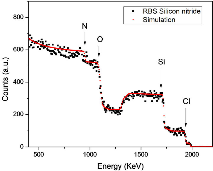
Figure 1. RBS spectrum of the sample M-50 after being annealed during 1 hour in an Ar athmosphere. The elements present in the sample are shown.
centrations of the elements that are present in both samples are shown in Table 1. The results show a decrement in chlorine amount as the ammonia flow rate increases; as well as a tendency to get an atomic composition near to that of stoichiometric silicon nitrides as larger ammonia flow rate are used during the preparation of the sample. This change in the films’ structure as a function of ammonia flow rate could be understood in terms of the hydrogen role during film formation. When enough hydrogen amount is in the chamber, silicon-nitride films are able to grow with low content of chlorine in their network, making them chemically more stable.
ERDA results are presented in Figure 2 and show the hydrogen amount in the samples. In any ERDA spectra the sample surface is located at higher energies, due to the energy loss of the projectiles as they interact with the atoms through the material. Figure 2 shows three curves that correspond to: 1) the reference sample (silicon wafer before the film was deposited) in green dots, 2) silicon nitride film deposited with 30 sccm NH3 flow rate (M-30) in red squares, and 3) silicon nitride film deposited with 50 sccm NH3 flow rate (M-50) in blue stars. Although the silicon wafer is hydrogen free, ERDA analysis detects a peak close to 1240 keV, which corresponds to a small amount of superficial hydrogen in the reference sample. This small amount of hydrogen can be due to handling and preparation of the samples, in which the surface can be contaminated with adsorbed hydrocarbons and vapor water. In the case of the other two curves, the

Table 1. Perecentage concentration of elements found in both samples.
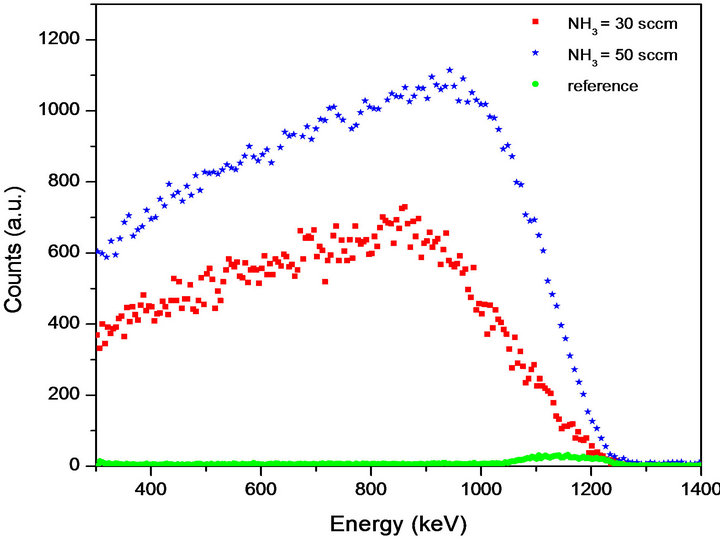
Figure 2. ERDA spectra of samples M-30 and M-50, as well as the reference sample (Si wafer). A large amount of hydrogen is observed for the samples containing a silicon nitride film.
continuum that extends to lower energies is typical of a constant bulk hydrogen concentration. This was verified by measuring spectra from Kapton, which has a constant hydrogen concentration, as well as from the SIMNRA simulations. Hydrogen was detected from the surface to 0.9 mm depth in both films, with concentrations of 4500 at/cm2 and 3200 at/cm2 for M-50 and M-30, respectively.
The first PL analyses were performed on the as-grown films, before they were irradiated with 8 MeV Si-ions. Some authors suggest that PL signals of silicon nitride films indicate the presence of nanocrystals in the matrix. This fact is due to that photoluminescence origin in these films is produced by a quantum confinement effect in the silicon nanoparticles embedded in nitride matrix [3,8]. Assuming an infinite potential barrier, and according to effective mass theory, when comparing the energy gap E of the confined Si-nc with that of the bulk silicon, an increased in E for the Si-nc is observed.
Others authors [1,2] also suggest that the increment in the energy of the band gap E is size depended. Quantum confinement theory assumes that the nanoparticle acts as a box of infinite walls with energy , where a is the size of the box. As the size of the nanoparticle increases, the energy decreases and an increment in the associated wavelength can be observed. This size dependence can be expressed as: [2]
 (1)
(1)
where Ebulk is the band-gap energy of the bulk crystal silicon, C is the quantum confinement parameter and d is average size of the silicon nanocluster (nm).
In this way, for Si-nc embedded in a silicon nitride matrix, E can be expressed as
 (2)
(2)
Figure 3 shows the PL spectra of samples M-30 and M-50, before they were irradiated with 8 MeV Si-ions. The figure shows two defined peaks at energies of 2.28 and 1.48 eV, respectively. A red-shift in the main PL

Figure 3. PL spectra of samples M-30 and M-50.
peak emission is observed as the hydrogen flow rate is increased. According to quantum confinement effect, the peaks represent the Si-nc embedded in the silicon nitride film. Using Equation (2), the mean size of Si-nc in M-30 is 3.24 nm; meanwhile, in M-50 is 6.07 nm.
The variation in particle size is expected, because as increasing the ammonia flow rate in the deposition chamber, a higher amount of hydrogen is produced during the growing process. As a consequence, a bigger concentration of hydrogen in the chamber could create nucleation sites in the material by breaking the Si-Si and Si-H bonds, with respect to the more stable Si-N or Si-Cl bonds [9]. This process also increases the density of silicon nanoparticles nucleation in the surface of the film and promotes the agglomeration of Si-nc during its growth [10].
In order to confirm the presence of Si-nc embedded in the as-grown silicon nitride films, HRTEM studied were performed.
Figure 4 shows HRTEM micrographs of both samples. Silicon nanoparticles appear as dark rounded spots, while the nitride silicon film appears as a lighter region surrounding the nanoparticles. At first sight it is observed that the sample M-50 deposited with 50 sc·cm NH3 flow rate (Figure 4(a)) show larger Si-nc than M-30 that was deposited at 30 sc·cm NH3 flow rate (Figure 4(b)). A statistical analysis of the HRTEM micrographs in different zones of the samples was performed in order to obtain the size distribution and the density of the Si-nc as precisely as possible. The results of these analysis show that the Si-nc size in the as-grown M-30 sample varies in the range from 2.0 nm to 4.2 nm, with an average size of 3.4 nm and a density of approximately 3.84 × 1011 cm−2; meanwhile in the as-grown M-50 sample, the size variation of the Si-nc, goes from 5.5 nm to 6.7 nm, with an average size of 6.3 nm and a density of approximately 6.76 × 1011 cm−2. A good agreement between the average sizes of the Si-nc obtained using the quantum confinement model for crystalline Si-nc and the ones measured from the HRTEM micrographs is observed. The difference in Si-nc density in both films can be explained as follows. For higher hydrogen concentration there would be more extraction of chlorine from the meta-stable SiClxHy [11], promoting the formation of HCl and leaving dangling bonds in the surface. This fact enhances the nucleation and growth of Si-nc in the film.
Once the samples were characterized, they were irradiated with 8 MeV Si-ions in order to observe the effect of the high energy silicon irradiation on the photoluminescence (PL) signal. The results are presented in Figures 5 and 6.
Figure 5 shows the PL signals of sample M-30 irradiated with 1 × 10¹⁴, 5 × 10¹⁴ and 1 × 10¹⁵ Si/cm2 fluencies. A blue shift relative to the as-grown sample is observed