Temporal Evolution of Anodization Current of Porous Silicon Samples ()
1. Introduction
Porous silicon is a material formed by anodic dissolution of single crystalline silicon in hydrofluoric acid (HF) solutions [1]. Recent porous silicon applications include: development of optical biosensors [2], detection of organic solvents [3], detection of organic vapors (methanol, ethanol, acetone and water) [4], among others.
The formation of porous silicon was first reported in the late 1950s as a result of electropolishing of silicon. Since then, particularly after 1990 when luminescence of porous silicon was discovered [5], extensive research had been undertaken [6-12]. Some of these investigations have revealed that porous silicon has many morphological features with properties that are very different from those of silicon. Also the formation process of porous silicon is very complex and it depends on many factors such as HF concentration, silicon type, current density, and illumination intensity. However, these studies have not revealed the mystery of the morphology variations and their effect on the thermal and electrical properties of the composite system silicon/porous silicon (Si/PSi).
In this work, a theoretical model that allows to analyze the anodization current as a function of the etching time of PS samples growth on (100) n-type silicon substrates with different resistivity values (r ~ 1 - 25 Wcm) is presented.
2. Experimental Setup
Porous silicon samples were obtained by using electrochemical etching of (100) n-type silicon wafers with different nominal resistivity values in the range (1 - 25 Wcm) (Mittel, Bromont-Ontario, Canada), see table 1 at room temperature in an electrolytic etching bath of 1:1 mixture of hydrofluoric acid (HF 48 wt%) and ethanol (96 wt%).
Most investigations related to porous silicon have been used galvanostatic anodization where the current intensity remains constant; however, the potentiostatic anodization which the anodization voltage is constant does not cause porous ramification during the growth process it assures the formation of the porous silicon with a more perfect and more uniform structure [13]. Furthermore, by means of potentiostatic anodization it is guaranteed that only one electrolytic process occur on the work electrode (silicon), but the reaction speed is generally small [14].
In this work the anodization was done potentiostatically with two voltage values (10 V and 20 V) and the etching time was 2 minutes under back illumination given by a laser with wavelength of 808nm (LASERMATE GROUP INC. Model LBG 8080250 A5-T). Platinum slab of high purity was used as cathode [15]. Figure 1 is a diagram of the experimental setup used in the sample fabrication.
The current data were collected using a multimeter Keithley 2000 with a GPIB universal serial bus (USB) connected directly to a personal computer.
3. Experimental Results
Figures 2 and 3 show the current as a function of etching time for different porous silicon samples that correspond to the wafers O1, O3 and O5. The samples O1A, O3A and O5A (see figures 2(a)-(c)) were produced with the anodization O5voltage equal to 10V, while the samples O1B, O3B and O5B (see figures 3(a)-(c)) with 20 V.
The current in all graphics of the figures 2 and 3 shows two different behaviors with the etching time. The first occurs at approximately 20 - 30 s and is related to the pore nucleation process. While the second corresponds to the remaining time and it is related to the porous growth process. These results concur to the stages of growth process as proposed by Kwon et al. [16] and Popkirov and Ottow [17]. In addition, it is observed that the current values increase when the substrate nominal resistivity is increased; this fact can be related with the electrochemical process that occurs in the interface between the substrate and the electrolytic solution.
4. Theoretical Model
When an n-type semiconductor is brought into contact with an electrolyte electrons will flow from the semiconductor to the solution phase. The resulting excess charge in the solid semiconductor does not reside at the surface as it would in a metal, but instead is distributed in a region near the surface called the space charge region [18]. At large scale, the space charge just acts as a series interface resistance [19].
During the pores formation process the effective resistance of the substrate changes continuously because the region that is in contact with the electrolytic solution
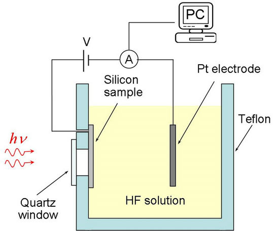
Figure 1. Diagram of the experimental setup.
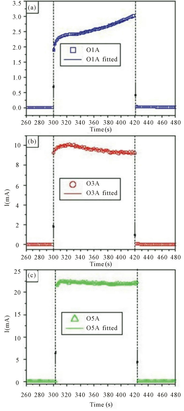
Figure 2. Current as a function of etching time for three different porous silicon samples using an anodization voltage of 10 V. (a) sample O1A (r ~ 1 - 5 Wcm), (b) sample O3A (r ~ 10 - 15 Wcm), (c) sample O5A (r ~ 20 - 25 Wcm). The symbols represent the experimental data, whereas the continuous lines the best theoretical fit obtained by means of the Equation (3). : applied voltage on;
 : applied voltage off. Dashed vertical lines were included to guide the eye.
is modified during the chemical reaction. The resistivity of the electrolyte penetrating inside the pores also varies because the local concentration of ions fluctuates [20,21].
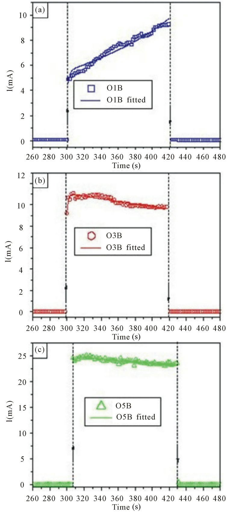
Figure 3. Current as a function of etching time for three different porous silicon samples using an anodization voltage of 20 V. (a) sample O1B (r ~ 1 - 5 Wcm), (b) sample O3B (r ~ 10 - 15 Wcm), (c) sample O5B (r ~ 20 - 25 Wcm). The symbols represent the experimental data, whereas the continuous lines the best theoretical fit obtained by means of the Equation (3). : applied voltage on;
 : applied voltage off. Dashed vertical lines were included to guide the eye.
In this work the system formed by the substrate and the substrate/electrolyte interface was modeled by means of two resistances connected in series that change in the time. The temporal variation of the effective resistance of the substrate is proposed as
 (1)
(1)
where rS and lm are the resistivity and the thickness of each substrate (see table 1), lp(t) is the pore depth and A(t) is the the chemically active area of the pore tip. The expression (1) is similar to the one presented by Christophersen et al. [22]. Due to the substrate thickness, lm, is much greater than the pore depth, lp(t), this last one can be rejected, i.e. lm-lp(t) ~ lm. For A(t) an exponential growth is proposed,  , where tS is a constant with time dimensions.
The equivalent resistance of the interface between the substrate and the electrolyte has been modeled by means of a lineal variation with the time,
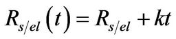 . (2)
. (2)
In the figures 2 and 3 the fitting of the experimental data have been included (continuous lines) modeling the current as
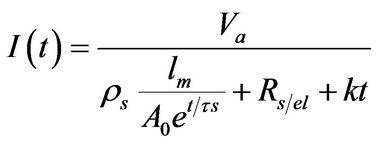 , (3)
, (3)
with Va the anodization voltage. The obtained values for the fitting parameters Ao, tS, RS/el and k are registered in table 2.
It is noteworthy that for the grown samples on the substrate with low resistivity value (wafer No. 1) the resis-
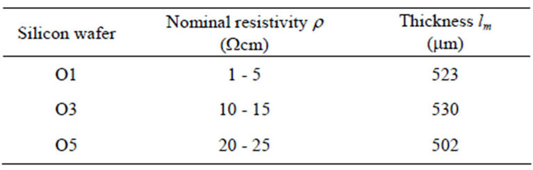
Table 1. Nominal resistivity and thickness values for the n-type silicon wafers.

Table 2. Value of the parameters Ao, tS, RS/el and k obtained by means of the fitting of the current graphs as a function of the etching time.
tance associated to the interface silicon/electrolyte diminishes for the two anodization voltages used (see the negative values of the parameter k). In addition, the value of the parameter RS/el for Va = 20V is smaller than the corresponding to Va = 10V, in contrast with the results obtained for the other porous samples corresponding to the wafers O3 and O5. These effects maybe can be related to the fact of having for the electrolyte a resistivity value (~4 Wcm) greater than the corresponding value of the wafer (~1 Wcm).
The resistivity of the hydrofluoric acid as a function of the concentration, for concentration values between 0 y 50 wt% 0˚C, is given by [23]
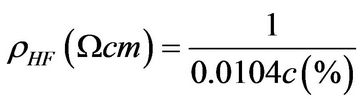 . (4)
. (4)
Due to the concentration of the hydrofluoric acid used in the electrolytic solution for the growth of the porous samples studied in this work was of 24 wt%, the resistivity of the electrolyte is obtained as 4 Wcm.
5. Conclusion
A simple theoretical model for the anodization current as a function of the etching time of porous silicon samples produced on n-type silicon substrates with different resistivity values was presented. The system formed by substrate and substrate/electrolyte interface was modeled through two resistances connected in series varying continuously in the time during the anodization process. By means of the fitting of the experimental data of the current as a function of the time with the proposed model, it is obtained that the existence of a correlation is probable between the resistivity values of the substrate and the resistivity of the electrolyte that does that the effective resistance of the substrate/electrolyte interface diminishes for the grown samples on the substrates of smaller resistivity studied in this research.
6. Acknowledgements
This work was partially supported by COLCIENCIAS, Universidad Nacional de Colombia and UNAM. Adriana Gutierrez wishes to thank COLCIENCIAS (Colombia) (Programa de Créditos Condonables para Doctorados Nacionales 2004) and Dirección Nacional de Investigación DINAIN, Universidad Nacional de Colombia (Colombia) for their support.
NOTES