A First Principles Simulation Framework for the Interactions between a Si(001) Surface and a Scanning Probe ()
1. Introduction
When silicon is cleaved in the (001) direction, each atom on the surface has two dangling bonds. In an attempt to reduce the surface energy, these atoms bond in pairs, forming dimers and by doing so eliminate one of the two dangling bonds per atom. It is well known that surfaces with buckled, asymmetric dimers have even lower surface energy compared to those with unbuckled, symmetric dimers. Depending on the buckling direction of the dimers, the following three reconstructed surfaces can be obtained: 1) p(2 × 1) surface which has all dimers buckled in the same direction; 2) p(2 × 2) surface with neighbouring dimers in each row buckled in the opposite direction and neighbouring dimers in a line normal to the dimer row are buckled in the same direction, and finally; 3) c(4 × 2) surface with neighbouring dimers buckled in alternating directions both along and normal to the dimer row.
Determining and manipulating arrangements of atoms on the Si(001) surface by a scanning probe microscopy (SPM) has been an ongoing issue for a long time. Experimental studies at low temperature using scanning tunnelling microscopy (STM) [1-3] and atomic force microscopy (AFM) [4,5] have shown that the c(4 × 2) geometry is the most stable of all possible reconstructions of the Si(001) surface. When the temperature is increased the c(4 × 2) arrangement of the buckled dimers becomes disordered and a new phase with p(2 × 1) periodicity is obtained. A reason for this is the “flip-flop” motion of the buckled dimers due to thermal excitation. Increasing the temperature, experiments with STM and AFM at room temperature resolve this surface with a symmetric p(2 × 1) structure [6,7]. Those observations are due to the thermally activated “flip-flop” motion of the dimers. Results from low energy electron diffraction show that an order-disorder phase transition takes place at temperatures of about 200 K [8]. Below this transition temperature the buckled dimers are stable in the c(4 × 2) ordering. Above the transition temperature the thermally activated dimer “flip-flop” motion results to the symmetric p(2 × 1) ordering. This dependence of the phase ordering on temperature has been long accepted until recent results obtained at sufficiently low temperatures at which it was believed a stable phase c(4 × 2) would be obtained, challenged that assumption. In particular these experiments showed that at temperatures as low as 5 K not only the c(4 × 2) phase can be observed, but other phases such as p(2 × 1) and p(2 × 2) can also be observed.
Indeed, observations made by an AFM by Suzuki et al. [4] involve images of the Si(001) surface at 120 K and 50 K [4] have found that the c(4 × 2) arrangements largely covered the scanning area at 120 K, however, when the temperature was decreased to about 50 K the area covered by p(2 × 2) increased. When lowering the temperature to 5 K and using the same AFM protocol, Uozumi et al. [5] observed asymmetric dimers with antiparallel “zigzag”-like patterns, a characteristic of the c(4 × 2) geometry, covered mainly the area. Two other arrangements, namely the p(2 × 2) and the p(2 × 1) were also observed. Further observations in STM experiments at low temperatures in the region of 20 K showed a symmetric p(2 × 1) structure. At such temperatures asymmetric dimers were only observed near defects [9]. The same mechanism was also obtained by Yokoyama et al. [7] using STM experiments at even lower temperatures in the region of 5 K. In these experiments they found out that the observation of symmetric p(2 × 1) structure was due to the anomalous dynamical flipping of the buckled dimers of c(4 × 2).
A number of research groups have performed experimental studies to explain the behaviour of atoms on the Si(001) surface induced by a scanning probe [3,10-12]. In such experiments they focused on three parameters that were known to affect the arrangement of atoms on the work surface, namely the bias voltage, the tunnelling current and the tip-sample interaction. All these experiments investigated the behaviour of Si(001) under different conditions using different protocols. However, they do not offer an explanation of this behaviour in the presence of the tip. It is thus highly desirable to develop first principles based modelling approaches to understand this behaviour of the Si(001) surface in the presence of a scanning probe and guide the design of experiments. It is therefore the aim of this paper to develop such a framework to simulate typical imaging protocols with SPM by systematically calculating tip-surface interactions along scanning probe trajectories and ultimately attempt to obtain a comprehensive understanding and a guideline for experiment design about how the tip affects the arrangement of atoms on the surface.
The tip-surface interaction has attracted much attention from the theoretical community aiming at explaining surface behaviour of different configurations of Si(001) surface [13-18]. Earlier theoretical work in this area has shown how covalent chemical interactions between the dangling bonds of the apex atom of a Si tip and the surface atoms introduce dominant forces which are responsible for atomic resolution and image contrast. Our previous results demonstrated that when the tip-surface distance is about 5 Å or higher, the chemical interaction between them is too weak therefore none of the atoms on the surface can be clearly imaged. By reducing the tipsurface distance to about 4 Å, its chemical interaction increases rapidly and atoms on the surface are clearly imaged. In addition it was shown how the direction of scanning plays an important role in observing atoms on the surface [17].
In this work we do not just perform calculations by placing the tip at just a few key positions over a confined model of a surface. We rather employ an extended surface in our model, not considered in earlier studies, and determine surface reconstructions as a function of tip position relative to the surface. Furthermore, scanning probe trajectories are simulated by advancing the tip in a stepwise manner as a real life tip would and perform quasistatic calculations to obtain force, energy landscape and surface reconstruction as explained in detail in the following section. These are key features of our modelling framework that can allow more faithful representation of real life scanning probe trajectories and by doing so provide better insight into the tip-surface interactions to inform imaging experiments. There is a distinctive gap in the literature as most theoretical work in this area is based on the approaches which involve considerably reduced size models and not tip trajectories mentioned earlier. We use our modelling framework to investigate the phase transitions that result from the interaction with the scanning probe, following typical trajectories above an asymmetric p(2 × 1) surface at a close distance to the surface. We extend our study to two additional surface reconstructions, namely the p(2 × 2) and c(4 × 2) surfaces, to provide a complete investigation and elucidate an understanding of how the probe manipulates atoms on the surface which have led to the observations made in experiments such as those by Sugimoto et al. [19-21].
2. Modelling and Computational Methodology
We consider a system comprising a Si(100) 2 × 1 slab and a Si tip. The tip was modeled as a single crystal Si comprising 4 Si atoms. The Si atoms at the base of the tip are saturated with H atoms and are kept fixed during calculations. Therefore there is a single dangling bond pointing downwards from the tip apex atom, towards the surface. This tip was chosen after results from total energy and normal force calculations obtained from this tip and another larger tip comprised of 10 Si atoms were almost the same, suggesting that the short range tip-surface interaction is dominated by the interaction of the dangling bond of the apex atom with the surface [16]. The slab is composed of a number of Si layers. The dangling bonds of the atoms at the bottom layer are saturated with H atoms. Each layer has 16 atoms, this means that when the surface is reconstructed there are 8 dimers arranged in two rows on the surface. The Si atoms on the bottom layer of the slab and the H atoms are always kept fixed during the calculations. The slab is chosen thick enough so that only atoms on the top layers can reconstruct and atoms on the lower layers remain at their bulk positions. Since we only consider tip-surface interactions and aim to completely avoid interaction between the tip and the bottom layers so in the supercell there is a vacuum gap between the tip and the bottom layer of the next supercell that is thick enough to avoid this interaction happening. Using a vacuum gap of 8 Å will satisfy that requirement. The unit cell which contains the slab, the tip and the vacuum gap is shown in Figure 1(a).
Throughout the calculations, total energy and atomic forces are calculated using density functional theory [22], which is implemented in the CASTEP code [23]. Results reported in [17] showed that in general both local density approximation (LDA) [24] and generalised gradient approximation (GGA) [25] for the exchange-correlation term for this system led to the same conclusion. Therefore in the present work we employ only the LDA method. Ultrasoft psuedopotentials are used for the electronion interaction. A plane-wave basis set for the electron wave function with cut-off energy of 450 eV is used. Integrations in the Brillouin zone are performed using special k-points generated with 2 × 2 × 1 Monkhurst-Pack grid. It is important to note that results such as total energy difference between different reconstructed surfaces, which we will show in the next section, are very close therefore special care was taken in using parameters such as energy cut-off, k-points etc. These values were chosen after extensive convergence calculations until final results were independent of the choice of those values. Atomic relaxations have been performed via a conjugate gradient scheme until the energy change (ΔE) between subsequent iterations of structural optimisation became less than 1 × 10⁻⁵ eV/atom, while the maximum forces (Fmax) acting on the atoms were less than 1 × 10⁻² eV/A. The energy tolerance (δE) between subsequent self-consistent iterations was less than 1 × 10⁻⁶ eV/atom.
Two modes of interaction between the tip and the surface are considered in this paper. The first mode is concerned with calculations at a fixed tip-surface distance of 4 Å—the vertical distance from the apex atom to the plane that contains adatoms, shown in Figure 1(a). At this tip-surface distance the interaction between them is dominated by the covalent chemical interaction which is responsible for atomic resolution and image contrast [16, 17,26]. The tip scans above dimers along the dimer line throughout the whole surface in steps of 0.5 Å. The second mode is concerned with calculations relating to vertical displacements of the tip from the vacuum region towards a lower atom of a dimer. In this mode each step takes place at 0.2 Å intervals. However, at tip-surface distances where dimers start to flip, for more accurate results, the simulation steps have a much shorter interval of 0.05 Å between them.
In each mode, total energies and normal forces are determined in a stepwise, quasistatic manner by making small movements of the tip either normal or parallel to the surface. At each step, the apex atom of the tip and atoms in the slab (except atoms on the bottom layer and H atoms which are kept fixed) are allowed to fully relax to their equilibrium positions for that particular tip position. The optimised surface structure obtained at the nth step is then used as an input (or “seed” structure) for the (n + 1)th step calculations.
3. Results and Discussion
3.1. p(2 × 1) to p(2 × 2) Phase Manipulation
In this section we report the results obtained when the tip scans across an asymmetric p(2 × 1) surface at a distance of 4 Å. The tip is displaced from region A to region B in three different scans, indicated by S1, S2, S3 in Figure 1(a). In Figure 1(b) we show a top-view for these three different scans over the first three layers. The results obtained from these scans are shown in Figures 2 and 3.
In scan S1 the tip is displaced from position A1 to position B1 as shown in Figure 2. Initially the tip is at position with coordinates (x, y, z) = (3.34 Å, 3.84 Å, 13.13 Å) with respect to the supercell’s coordinate frame. At this position of the tip the interaction between the tip and
 (a) (b)
Figure 1. (a) A ball-and-stick model of the structures of the Si(001)-p(2 × 1) surface and the silicon scanning probe, with H atoms represented by the brighter coloured spheres. Indexes S1, S2, S3 indicate three different scans from region A to region B. Indexes 1, 2, ···, 11 represent different atom positions of the first 6 layers, the same representations are also used in Figures 3, 4 and Tables 1, 2; (b) Top-view of the first 4 layers of the p(2 × 1) structure (here we separate the first layer into two layers, one layer for adatoms and the other for lower atoms), different ball sizes represent Si atoms in different layers.
the lower atom of coordinates (x, y, z) = (4.94 Å, 3.84 Å, 8.42 Å) is still too weak to cause the dimer to flip. When the tip translates further for about 0.5 Å along the direction of the scan, there is a strong attractive force between the apex atom of the tip and that lower atom, causing it to move up towards the tip. At this position the dimer starts to flip.
Once the dimer flips to its new configuration, it remains in this configuration for the duration of the scan thus deforming the surface to this configuration permanently. It remains in this configuration even when the tip is above the “new” lower atom. This behaviour can be explained as follows: when the dimer flips the total energy is lowered by 0.17 eV compared to that before flipping taking place. This value is obtained by an optimisation calculation for a p(2 × 1) surface without the presence of the probe but having one flipped dimer. This implies that, when the tip is above the “new” lower atom, in order to cause the dimer to flip back to its original configuration, it requires an energy gain that exceeds 0.17 eV. However, with the presence of the probe at a distance of 4 Å above the surface, or 4.7 Å above the “new” lower atom, the energy input into the system as a result of the interaction between the tip and the surface is only 0.11 eV. This energy gain is not strong enough to overcome that barrier and cause the dimer to flip back to its original configuration.
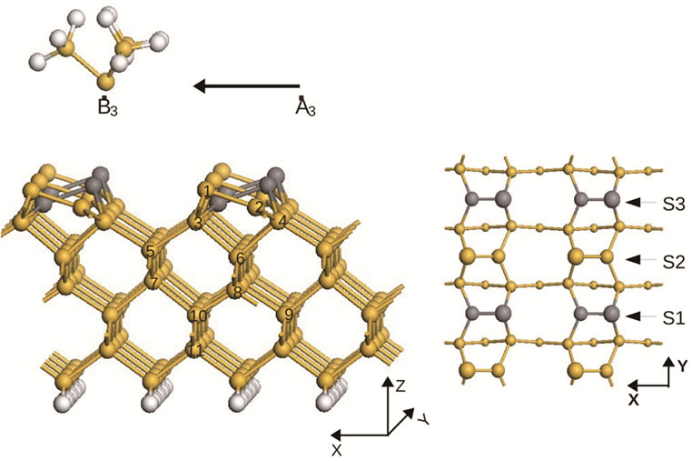
Further along the scan direction closer to the next row in region B, in particular position B1 in Figure 2, the dimer there flips too when the the tip is above the lower atom of that dimer. This dimer also remains in its new
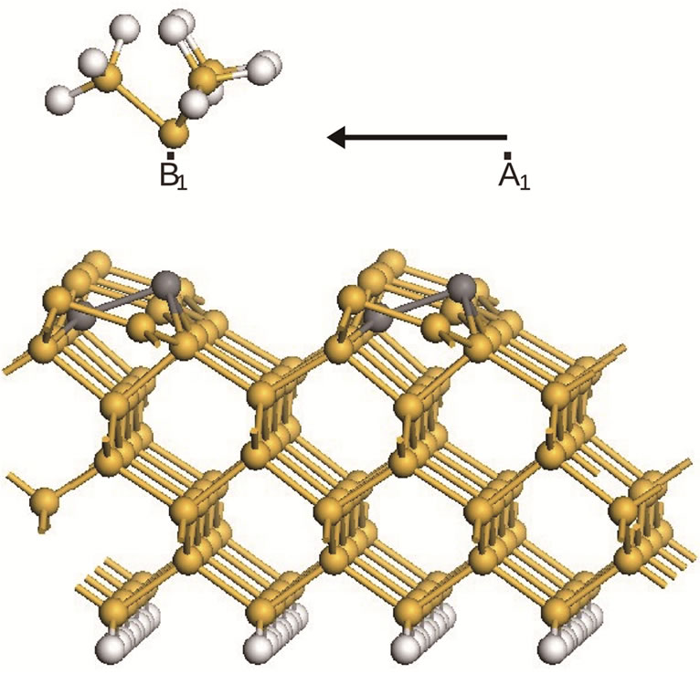
Figure 2. The surface structure at the end of the first scan (S1), from A1 to B1. The newly flipped dimers are presented in the dark-gray balls.
configuration even when the tip is displaced further away from the dimer along the scan direction. It is important to note that the dimer in the second row starts to flip even at a position of the tip at 10.94 Å along the x direction and as far as ~1.7 Å laterally ahead the lower atom at 12.63 Å along the x direction. This position of the tip is much further away from the lower atom, about 0.6 Å, than the position of the tip with respect to the lower atom in the first row at which the dimer flips. This difference is due to the fact that the system is more stable when dimers in the same row are oriented in alternation in opposing directions. When a dimer in the second row flips not only it lowers the surface energy by orientating opposite to the dimers next to it but also forms with the flipped dimers in the first row a local p(2 × 2) structure which is more stable than the p(2 × 1) structure. One can conclude that in a p(2 × 1) surface a flipped dimer lowers the energy barrier to flipping the dimer next to it in the next row compared to that of a perfect p(2 × 1) surface.
The next scan, labeled as S2, represents the displacement of the tip from position A2 to position B2 shown in the Figure 1(a). Throughout this scan no dimer flipping takes place. The reason is that the energy required to excite the dimer and cause it to flip is greater in the p(2 × 2) surface compared to that in the p(2 × 1) surface. However, at a tip-surface distance of h = 4 Å the interaction between the tip and the surface is too weak to overcome the energy barrier to the onset of flipping in the local p(2 × 2) structure.
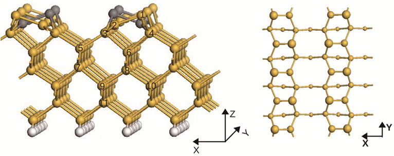
In the final scan S3, which represents a translation of the tip from position A3 to position B3 (shown in Figure 3), flipping of the dimer does occur when the tip scans over the lower atoms. This is the same behaviour as in the first scan S1. In this scan flipping takes place when the tip is at a position with coordinates (3.34 Å, 11.52 Å, 13.13 Å)—at about 1.6 Å along the x direction and above the lower atom with coordinates (4.94 Å, 11.52 Å, 8.42 Å). So it clearly shows that the first toggled dimer in the scan S1 not only affects, reduces the toggling energy barrier, for the immediate neighbouring dimer in the adjacent row but also to the following nearest neighbouring dimers on the same row.
After the tip has scanned the whole surface a complete phase transition from p(2 × 1) to p(2 × 2) takes place as shown in Figure 3. A structural optimisation is performed for this surface without the tip to calculate the energy gain per dimer as a result of the transition from p(2 × 1) to p(2 × 2) structures. Following these calculations it can be confirmed, that the p(2 × 2) structure is more stable than the asymmetric p(2 × 1) structure with an energy-per-dimer difference between these two surfaces of about 0.062 eV. However this p(2 × 2) structure is not yet the ground state of Si(001). Indeed, by flipping all dimers in one row of the p(2 × 2) surface and then performing an optimisation calculation, the c(4 × 2) surface is obtained, shown in Figure 4. The calculations show that this is the most stable surface of Si(001). The energy per dimer of this surface is 3 meV lower than that of the p(2 × 2) surface. Our results confirm the computational results obtained by other groups [15,18].
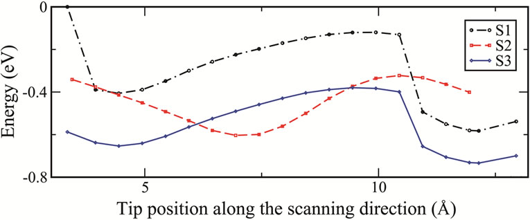
From an AFM imaging point of view, it has been shown that in lateral scans the variations of the energy and the force have the same trend and the energy or the force distribution can be considered as a qualitative prediction of the AFM image in the frequency shift mode [16,17]. In Figure 5 the total energy and the normal force as functions of the tip positions are shown as the tip translates along the direction of the scan from region A to B as discussed above. The force at each scanning step is calculated by summing the forces on all fixed atoms
 (a) (b)
Figure 3. (a) The surface structure at the end of the third scan (S3), from A3 to B3. In this scan we observe again dimer flipping. The newly flipped dimers, together with the ones previously flipped in scan S1, are shown as dark gray balls. At the end of this scan the structure has completely transformed into a new structure, the Si(001)-p(2 × 2) structure. This new surface remains stable even after the scanning probe is completely retracted; (b) Top-view of the first 4 layers of the p(2 × 2) structure (here we separate the first layer into two layers, one layer for adatoms and the other for lower atoms).
 (a) (b)
Figure 4. (a) A new surface is obtained after all dimers in one row are flipped and then structural optimisation is performed. The new surface obtained is the Si(001)-c(4 × 2); (b) Top-view of the first 4 layers of the c(4 × 2) structure.
 (a)
(a)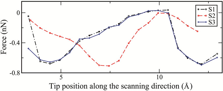 (b)
(b)
Figure 5. (a) Total energies and (b) normal forces as functions of tip position along the scanning direction for each of the three different scans.
(H and Si atoms) of the tip. From these curves we clearly see that the energies and the forces follow a similar trend and are nearly the same for both S1 and S3 scans. They have a minimum in energy (or maximum in the normal force) when the tip is above the lower atom of the dimer causing it to flip. When the dimer flips, the lower atom which now becomes the adatom is closer to the tip. The strong interaction between them results to the maximum in the normal force. In scan S2 there is no dimer flipping therefore the strongest interaction occurs when the tip is above the adatoms of the dimmers.
3.2. Comparison of p(2 × 1), p(2 × 2) and c(4 × 2) Surfaces
Bond lengths of dimers and back bonds, as well as buckling for the first 6 layers of three different surfaces obtained in our work are shown in Tables 1 and 2. Results obtained from experimental observations [27,28] are included for comparison. In general, our results are in agreement with results obtained by those groups. In particular dimer bond lengths, buckling heights—or buckling angles—of p(2 × 2) and c(4 × 2) are nearly the same with small differences by only a few percent.
The lengths between a topmost atom on the first layer of the surface and atoms on the layers beneath it are in very good agreement between our results and the results obtained by LEED experiments [27,28]. In Table 2 we show buckling lengths for atoms labeled from 1 to 11 in the 6 layers of three different surfaces obtained in our work and compared to those obtained by LEED experiments [27,28]. These are the lengths between each atom
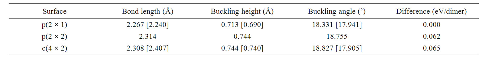
Table 1. Bond-length, buckling height, buckling angle between 2 atoms of a dimer for three different reconstructed surfaces obtained in this work and compared to the experimental results in [27,28] (shown in square brackets). The energy difference per dimer between p(2 × 1) and the other surfaces is also shown.
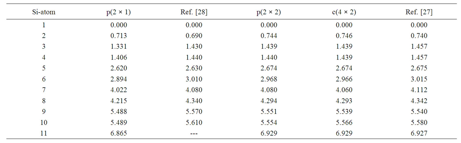
Table 2. Z-coordinate of Si atoms for the reconstructed Si(100)-p(2 × 1), p(2 × 2), c(4 × 2) surfaces obtained by our calculations and compared with LEED measurements [27,28]. The numbers on the far left column represent the labels of different atom positions of the first 6 layers. The same labels are also used in Figures 1, 3, 4.
labeled 2 to 11 and atom labeled 1. The labels from 1 to 11 are also shown in Figures 1, 3 and 4. Most of the atoms on these layers for these three surfaces are buckled in the same way except atoms on the second and the fifth layers. On the fifth layer, there is a similar ordering of atoms labeled 9 and 10 in p(2 × 1) and p(2 × 2), but in c(4 × 2) the ordering of atoms labeled 9 and 10 is reversed from that of p(2 × 1) or p(2 × 2). However, in the fifth layer towards the inner layers, atoms buckled relative to its bulk positions are very small and can be neglected. In the second layer, it is interesting to observe the similarity between p(2 × 2) and c(4 × 2) structures and how they differ to the p(2 × 1) structure. In p(2 × 2) or c(4 × 2) structures there is virtually no buckling between atoms labeled 3 and 4. This could be due to the fact that dimers on the first layer are arranged alternatively in opposite directions hence it compensates for each other and does not favourably induce any atom below it to be buckled. However, in the p(2 × 1) case atoms on second layer are buckled by 0.1 Å, this small buckling is due to the buckled dimerization in the first layer.
3.3. Surface Manipulations with Vertical Tip Displacements
In the previous sections we discussed that an external energy which is sufficient to overcome an energy barrier is required to cause a dimer in a p(2 × 1) surface to flip. During an AFM scan, this external energy is provided by the scanning probe when it is sufficiently close to the surface. There is a certain distance between the scanning probe and the surface at which the interaction is strong enough to overcome the energy barrier and flip the dimer. To determine this distance, the energy and the force are obtained by translating the tip in steps of 0.2 Å from the vacuum region where there is no tip-surface interaction towards the lower atom of a dimer in each of the three surfaces, p(2 × 1), c(2 × 2) and c(4 × 2) (see Figure 6). In the region where dimers undergo flipping the distance between each step is reduced to 0.05 Å. Without loss of generality, the system considered in these calculations is reduced to a unit cell comprising 4 dimers arranged in two rows.
The results show that, for the p(2 × 1) surface the dimer flips when the tip is at a distance h ~ 4.10 Å. For p(2 × 2) and c(4 × 2) surfaces flipping occurs at distances h ~ 3.90 Å and 3.80 Å, respectively. At those distances h for each of those surfaces the energies due to the tipsurface interactions that overcome the energy barriers are 0.207 (eV), 0.268 (eV) and 0.318 (eV), respectively. It therefore demonstrates that tip-surface distance h at which a dimer flips in the p(2 × 1) surface is higher than that of p(2 × 2) and c(4 × 2). Thus, for ,
,  and
and  being the critical tip-surface distances for these three surfaces at which dimers flip, one can observe that
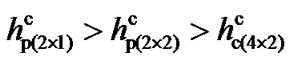 . Similarly, for
 ,
, and
and  being the energy barriers then
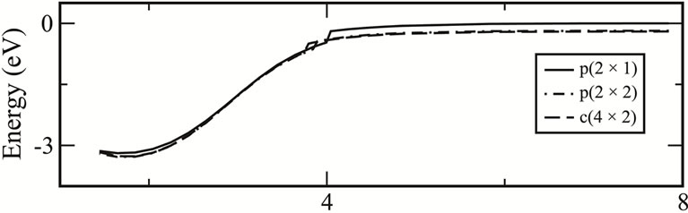
 . This result is in agreement with results by Kantorovich et al. [15] which were obtained by constrained energy minimization calculations. Furthermore, it is worthwhile noting the hysteresis in the energy and normal force curves when the tip is at the threshold distance above a lower atom, Figures 6(a) and (b). At this threshold, a sudden increase in the tip-surface interaction occurs as the lower atom moves closer to the tip during dimer flipping. Meanwhile, when the tip scans perpendicularly in an attractive region above an adatom no dimer flipping takes place therefore no hysteretic behaviour is observed in this scan. This behaviour can be seen in Figure 6(c) showing the energy curve during vertical tip displacements above an adatom.
In Figure 7 we show different surface structures obtained at different tip heights, h, above a lower atom for all three surfaces considered in this paper. At h = 8.0 Å there is no interaction between the tip and the surface, therefore the energy of the system is calculated by a straightforward summation of energies of the tip and the surface. As the tip is brought closer to the surface at a distance h = 3.4 Å, dimer flipping does take place in all surfaces considered. At this distance we observe similar behaviour in all surfaces where dimers in one row buckled in the same direction while dimers in other rows buckled in opposite directions in alternation. This results
 (a)
(a)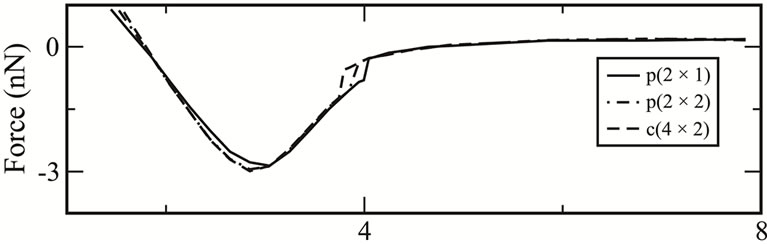 (b)
(b)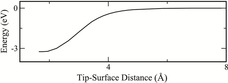 (c)
(c)
Figure 6. (a) Total energies and (b) normal forces as functions of tip-surface distance, h, when the tip is displaced vertically from the vacuum region towards the lower atom of a dimer for each of the three different surfaces p(2 × 1), p(2 × 2), c(4 × 2); (c) Energy curve when the tip scans vertically above an adatom in the p(2 × 1).
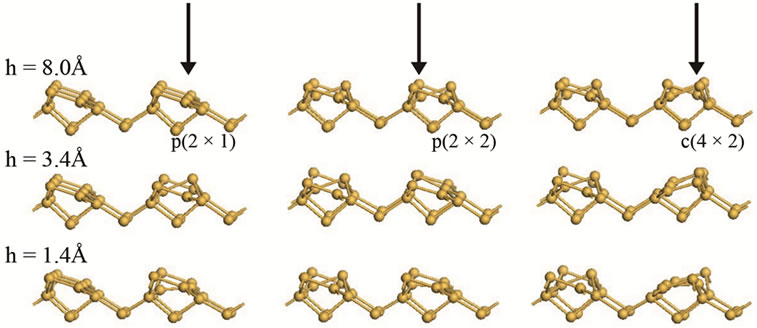
Figure 7. Surface structures of p(2 × 1), p(2 × 2), c(4 × 2) at various tip-surface distances, h, when the tip is displaced vertically from the vacuum region towards a lower atom. The direction of the scan is denoted by the arrows.
to an equal in energy in all surfaces, as can be seen in Figure 6(a) for h in the region of 3.4 Å. Further reduction of h to 1.4 Å there is a repulsive interaction between the tip and the surface. In this case we can observe that the adatom below the tip is pushed downwards leading to a symmetric dimer. The same behaviour was observed by Cho et al. [13].
4. Conclusions
In this paper we presented a modelling framework that employes total energy calculations to study the interactions between a Si tip and surface. With this framework we conducted a systematic study of the phase transitions from p(2 × 1) to p(2 × 2) reconstructions which are the result of the interactions between the surface and the Si scanning probe. In the simulations the tip scans along an initial p(2 × 1) surface at a constant height of 4 Å above the surface. The tip scans the surface in a direction normal to the dimer rows. As a result of the interactions between the tip and the surface the dimers along the first scan toggle and locally form a p(2 × 2) structure. The formation of the p(2 × 2) structure reduces the total energy of the system and increases the energy barrier that prevents the surface to form its original configuration, causing a permanent deformation of the surface. During the second scan along the next dimer line, which has a local configuration of p(2 × 2), no dimer flipping is observed. This is due to the tip-surface interaction is not strong enough to overcome the energy barrier required to cause the dimer to flip. In a third scan over the next dimer line which has a local p(2 × 1) structure, dimer flipping is observed again. After the tip has completely scanned the surface, a complete phase transition from p(2 × 1) to p(2 × 2) has taken place with an energy per dimer of the p(2 × 2) structure being lower than that of the p(2 × 1) structure by 0.062 eV.
Furthermore, the relationship between the total energy and the normal force at specific tip-surface distances, h, are calculated for the three different surface reconstructions. In our calculations we found that the critical value of the tip-surface distance, at which the tip causes the dimers to flip, is higher for the p(2 × 1) structure than that of the p(2 × 2) and c(4 × 2) structures. It thus follows that the energy barrier is lower for the p(2 × 1) structure than that of the p(2 × 2) and c(4 × 2) structures. These results provide an understanding of the behaviour of the Si(001) surface when a tip is present and can therefore provide a guideline in designing experimental protocols involving atomic manipulations with SPM on this type of surface such as those pioneered by the groups of Sugimoto et al. [19,21] and Oyabu et al. [29-31]. Finally, with the capability of modern instruments to control with atomic precision tip trajectories and with future modelbased support using simulation frameworks such as the one described here, one can envisage that scanning probes can be used as a tool not only to manipulate atoms on the surface but also to “pick and place” single atoms or small molecules and grow almost any arbitrary structure on a given surface in the future [32].
5. Acknowledgements
This work has been supported by the UK Engineering and Physical Sciences Research Council (EPSRC) under contract EP/F009801/1 and Brunel University’s BRIEF award scheme. The authors would like to thank the School of Engineering and Design for purchasing our computing cluster to support research in this area. All simulations were performed on the cluster comprising 64 processors at Brunel University.
NOTES