Journal of Materials Science and Chemical Engineering
Vol.05 No.01(2017), Article ID:73253,11 pages
10.4236/msce.2017.51003
TEM Observation of Si0.99C0.01 Thin Films with Arsenic-Ion-, Boron-Ion-, and Silicon-Ion-Implantation Followed by Rapid Thermal Annealing
Junji Yamanaka1, Shigenori Inoue1, Keisuke Arimoto1, Kiyokazu Nakagawa1, Kentarou Sawano2, Yasuhiro Shiraki2, Atsushi Moriya3, Yasuhiro Inokuchi3, Yasuo Kunii3
1Center for Crystal Science and Technology, University of Yamanashi, Kofu, Japan
2Advanced Research Laboratories, Tokyo City University, Tokyo, Japan
3Hitachi Kokusai Electric Inc., Toyama, Japan


Received: November 11, 2016; Accepted: January 1, 2017; Published: January 4, 2017
ABSTRACT
Strained Si and its related materials, such as strained SiGe and strained silicon-carbon alloy (Si-C), are receiving tremendous interest due to their high carrier mobility. In this study we carry out a basic investigation of the change in microstructure of ion-implanted Si-C solid solution caused by rapid thermal annealing, because it is very important to realize a field-effect transistor made of this new material. The microstructures of arsenic-ion-, boron-ion-, and silicon-ion-implanted Si0.99C0.01 specimens upon thermal annealing are observed using transmission electron microscopy, and it is revealed that the rate of solid-state crystallization of ion-implanted Si-C is slower than that of the ion-implanted Si.
Keywords:
Strained Heterodevice, Silicon-Carbon Alloy, Ion Implantation, Transmission Electron Microscopy

1. Introduction
Si-based strained heterostructures are attracting tremendous interest because of their potential for high-speed devices. For example, it has been reported that strained Si exhibits high carrier mobility [1] [2] [3] [4]. Many researchers, including ourselves, have proposed various methods of producing strain-relaxed SiGe as a virtual substrate for strained Si [5]-[19]. The technology of stained- Si/SiGe is now expected be applied to a practical device-producing processes.
At present, the technologies of other strained heterostructures such as strained- SiGe/Si and strained-(Si-C)/Si are still being developed. We still need to conduct basic research on these technologies which has been carried out by many researchers [20]-[29]. In particular, it is necessary to study the thermal stability of Si-C because the solid solution of Si-C is not thermodynamically stable [30] [31]. Specifically, the study of impurity-doped Si-C is very important for the realization of a field-effect transistor (FET).
As a basic study for future applications, we investigated the recrystallization behavior of arsenic-ion-, boron-ion-, and silicon-ion-implanted Si0.99C0.01 by trans- mission electron microscopy (TEM). Arsenic and boron were selected because of their practical importance. Silicon, which is the matrix material of the target Si0.99C0.01 film, was selected to clarify the effect of ion-implantation.
2. Experimental Procedure
80-nm-thick Si0.99C0.01 films were epitaxially grown on p-type Si (100) wafers by chemical vapor deposition. We then prepared arsenic-ion-implanted, boron- ion-implanted, and silicon-ion-implanted specimens. Ion-implantation conditions were selected so that the ion distributions were similar. The ion source, acceleration voltage, and ion dose of each specimen are shown in Table 1.
Each specimen was then annealed at a temperature of 800˚C or 1000˚C for 60 s in a rapid thermal annealing (RTA) system in an atmosphere of argon. X-ray reciprocal space mapping (X-ray RSM) was utilized to evaluate the lattice strain and carbon composition. TEM specimens were prepared by an argon ion-mil- ling process with an acceleration voltage of 4 kV. After that, the microstructures of the specimens were observed by TEM using a conventional filament-type microscope (JEOL JEM-2000FX-II). For comparison, we also carried out the arsenic-ion implantation and annealing of a p-type Si (100) wafer.
3. Results and Discussion
The ion ranges were simulated using TRIM, a well-known ion-implantation program, the results of which are shown in Figure 1 [32] [33]. These results show that we can expect similar ion distributions in all the prepared specimens. Specifically, the amorphous phase may be produced below the surface with a depth of several tens of nm.
Figure 2 shows the result of TEM observation of the arsenic-ion-implanted Si.
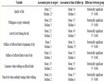
Table 1. Ion implantation conditions.
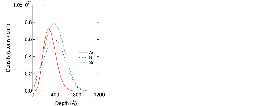
Figure 1. Simulated ion distributions calculated using TRIM [32] [33].
Figure 2(a) shows a cross-sectional bright-field image (BFI) of the arsenic-ion- implanted Si. There is no contrast from the surface to a depth of about 60 nm. Therefore, it is considered that an amorphous Si layer with a thickness of about 60 nm was formed below the surface. There is a diffraction contrast at a greater depth, as shown in Figure 2(a), indicating a crystalline structure. Figure 2(b) shows a cross-sectional BFI of arsenic-ion-implanted Si after annealing at 800˚C for 1 min, showing that the amorphous region was completely recrystallized to a single crystal, although it included some lattice defects. Figure 2(c) shows a BFI of arsenic-ion-implanted Si after annealing at 1000˚C for 1 min; the crystallinity of this specimen is almost perfect.
The substitutional carbon composition of the silicon-carbon thin film deposited on a Si substrate by CVD was evaluated using the result of X-ray RMS, which is not shown here, and it was approximately 1 atom%. Figure 3(a) and Figure 3(b) show a bright-field TEM image and diffraction pattern of as-depo- sited Si0.99C0.01, respectively. There is no evidence of lattice defects in Figure 3(a) and only the diffraction spots of the Si0.99C0.01 film and Si substrate can be seen in Figure 3(b). These results show that we succeeded in producing a single-crystal Si0.99C0.01 solid solution film on the Si substrate.
Figure 4 and Figure 5 show the result of TEM observation of arsenic-ion- implanted Si0.99C0.01. Figure 4(a) shows a BFI of as-implanted Si0.99C0.01, which shows that a layer of Si0.99C0.01 of approximately 55 nm thickness became amorphous upon arsenic-ion implantation. This behavior is almost the same as that of Si, which is shown in Figure 2(a).
On the other hand, the crystallization behaviors of arsnic-ion-implanted Si0.99C0.01 and arsenic-ion-implanted Si, which are shown in Figure 2, were completely different as mentioned below. Figure 4(b) shows a BFI of arsenic-ion- implanted Si0.99C0.01 after annealing at 800˚C for 1 min. This annealing condition is identical to that for Si, the result of which is shown in Figure 2(b); however, a very wide amorphous region remains in Si0.99C0.01. Figure 4(c) shows a BFI of arsenic-ion-implanted Si0.99C0.01 after annealing at 1000˚C for 1 min.

Figure 2. TEM observation of arsenic-ion-implanted Si. (a) Cross-sectional bright-field image (BFI) of arsenic-ion-implanted Si. (b) Cross-sectional BFI of arsenic-ion-implanted Si after annealing at 800˚C for 1 min. (c) BFI of arsenic-ion-implanted Si after annealing at 1000˚C for 1 min.
In this case, there was no residual amorphous region in Si0.99C0.01, although the single crystal Si0.99C0.01 layer contained many defects. Figure 4(d) shows a SADP corresponding to the BFI in Figure 4(c). Diffraction spots originating from twins can be clearly seen. The high-resolution lattice image (Figure 5) also shows that the specimen contains many defects and has large numbers of twins and stacking faults.
Figure 6 shows the result of TEM observation of boron-ion-implanted Si0.99C0.01. Figure 6(a) shows a BFI of as-implanted Si0.99C0.01, which shows that a layer of

Figure 3. TEM observation of as-deposited Si0.99C0.01. (a) Cross-sectional BFI. (b) Selected-area electron diffraction pattern (SADP).
Si0.99C0.01 of approximately 70 nm thickness became amorphous upon boron-ion implantation. This result is similar to those for the arsenic-ion-implanted Si0.99C0.01 and Si. However, the rate of solid-state crystallization of boron-ion- implanted Si0.99C0.01 is slower than that of ion-implanted Si. Figure 6(b) shows a BFI of boron-ion-implanted Si0.99C0.01 after annealing at 800˚C for 1 min. An amorphous region remains below the surface, although the region is smaller than that for the arsenic-ion-implanted specimen after annealing, which is shown in Figure 4(b). Figure 6(c) shows a BFI of boron-ion-implanted Si0.99C0.01 after annealing at 1000˚C for 1 min. The Si0.99C0.01 was fully crystallized but it contained many defects, similarly to the arsenic-ion-implanted Si0.99C0.01 shown in Figure 4(c).
Through the results for arsenic-ion-implanted Si0.99C0.01 and boron-ion-im- planted Si0.99C0.01, it is clear that the recrystallization behavior of ion-implanted Si0.99C0.01 is different from that of ion-implanted Si. However, it is difficult to clarify the physical origin of this phenomenon because it is a result of many complex factors. Therefore, we carried out experiments on silicon-ion-implanted Si0.99C0.01, because silicon is the matrix element of the thin film; thus, it is not necessary to consider the chemical interaction between the implanted element and

Figure 4. TEM observation of arsenic-ion-implanted Si0.99C0.01. (a) BFI of as-implanted Si0.99C0.01. (b) BFI of arsenic-ion-implanted Si0.99C0.01 after annealing at 800˚C for 1 min. (c) BFI of arsenic-ion-implanted Si0.99C0.01 after annealing at 1000˚C for 1 min. (d) SADP corresponding to the BFI in Figure 4(c).
the elements of the films, Si and C.
Figure 7 shows the result of TEM observation of silicon-ion-implanted Si0.99C0.01. Figure 7(a) shows a BFI of as-implanted Si0.99C0.01, which shows that a

Figure 5. High-resolution lattice image of arsenic-ion- implanted Si0.99C0.01.
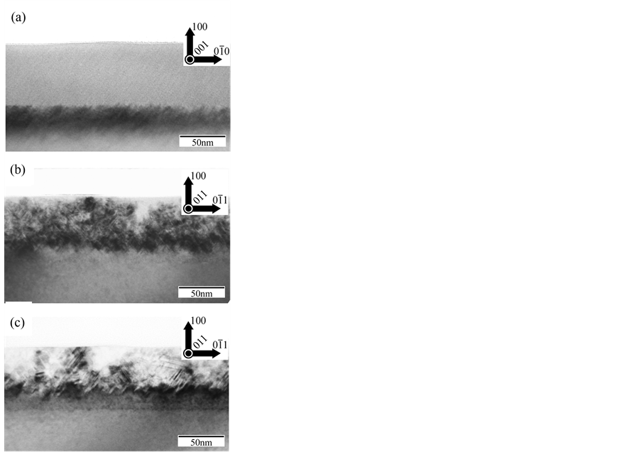
Figure 6. TEM observation of boron-ion-implanted Si0.99C0.01. (a) BFI of as-implanted Si0.99C0.01. (b) BFI of boron-ion-implanted Si0.99C0.01 after annealing at 800˚C for 1 min. (c) BFI of boron-ion-implanted Si0.99C0.01 after annealing at 1000˚C for 1 min.

Figure 7. TEM observation of silicon-ion-implanted Si0.99C0.01. (a) BFI of as-implanted Si0.99C0.01. (b) BFI of silicon-ion-implanted Si0.99C0.01 after annealing at 800˚C for 1 min. (c) BFI of silicon-ion-implanted Si0.99C0.01 after annealing at 1000˚C for 1 min.
layer of Si0.99C0.01 of approximately 65 nm thickness became amorphous upon silicon-ion implantation. Figure 7(b) shows a BFI of silicon-ion-implanted Si0.99C0.01 after annealing at 800˚C for 1 min. A very wide amorphous region remains in the Si0.99C0.01, similarly to the case of arsenic-ion-implanted Si0.99C0.01. Figure 7(c) shows a BFI of silicon-ion-implanted Si0.99C0.01 after annealing at 1000˚C for 1 min. In this case, the Si0.99C0.01 was fully crystallized but it contained many defects similarly to the cases of arsenic-ion-implanted Si0.99C0.01 and boron-ion-implanted Si0.99C0.01.
The result for the silicon-ion-implanted specimen was very similar to those for the arsenic-ion-implanted and boron-ion-implanted specimens. This fact leads us to the conclusion that the chemical interaction between the doped elements and Si and/or C is not the main reason for the difficulty of forming defect-free single-crystal Si0.99C0.01 by solid-phase crystallization. Our experimental results suggest that the carbon atoms themselves might play a role in the inhibition of recrystallization.
4. Summary
We produced a single-crystal Si0.99C0.01 solid solution film on a Si substrate and implanted arsenic ions, boron ions, and silicon ions into the specimens. We then annealed the specimens by RTA and observed the microstructures of the specimens by TEM. It was revealed that the rate of recrystallization of ion-implanted Si0.99C0.01 is slower than that of ion-implanted Si. Furthermore, the crystallinity of Si0.99C0.01 was inferior to that of Si, even after Si0.99C0.01 was fully crystallized. Therefore, further basic research on the solid-phase crystallization of Si0.99C0.01 is necessary to promote the realization of future applications. The precise mechanism of solid-phase crystallization of Si0.99C0.01 is still under discussion at this stage; however, we revealed that the interaction between arsenic/boron and Si/C did not directly affect this phenomenon because the silicon-ion-implanted specimen showed the same results to arsenic-ion-implanted and boron-ion-im- planted specimens. It is concluded that the carbon atoms in the specimen play a role in inhibiting the recrystallization.
Acknowledgements
The authors thank Mr. Motoki Sato, Mr. Kazutoshi Nagayoshi and Ms. Chiaya Yamamoto of the University of Yamanashi for their help in experiments.
Cite this paper
Yamanaka, J., Inoue, S., Arimoto, K., Nakagawa, K., Sawano, K., Shiraki, Y., Moriya, A., Inokuchi, Y. and Kunii, Y. (2017) TEM Observation of Si0.99C0.01 Thin Films with Arsenic-Ion-, Boron-Ion-, and Silicon-Ion-Implantation Followed by Rapid Thermal Annealing. Journal of Materials Science and Chemical Engineering, 5, 15-25. http://dx.doi.org/10.4236/msce.2017.51003
References
- 1. Mii, Y.-J., Xie, Y.-H., Fitzgerald, E.A., Monroe, D., Thiel, F.A., Weir, B.E. and Feldman, L.C. (1991) Appl. Phys. Lett., 59, 1611. https://doi.org/10.1063/1.106246
- 2. Ismail, K., LeGoues, F.K., Saenger, K.L., Arafa, M., Chu, J.O., Mooney, P.M. and Meyerson, B.S. (1994) Phys. Rev. Lett., 73, 3447. https://doi.org/10.1103/PhysRevLett.73.3447
- 3. Sugii, N., Nakagawa, K., Kimura, Y., Yamaguchi, S. and Miyao, M. (1998) Jpn. J. Appl. Phys., 37, 1308. https://doi.org/10.1143/JJAP.37.1308
- 4. Xie, Y.H., Monroe, D., Fitzgerald, E.A., Silverman, P.J., Thiel, F.A. and Watson, G.P. (1993) Appl. Phys. Lett., 63, 2263. https://doi.org/10.1063/1.110547
- 5. Meyerson, B.S., Uram, K.J. and LeGoues, F.K. (1988) Appl. Phys. Lett., 53, 2555. https://doi.org/10.1063/1.100206
- 6. Mooney, P.M., Jordan-Sweet, J.L., Ismail, K., Chu, J.O., Feestra, R.M. and LeGoues, F.K. (1995) Appl. Phys. Lett., 67, 2373. https://doi.org/10.1063/1.114349
- 7. Chen, H., Guo, L.W., Cui, Q., Hu, Q., Huang, Q. and Zhou, J.M. (1996) J. Appl. Phys., 79, 1167. https://doi.org/10.1063/1.360899
- 8. Li, J.-H., Peng, C.S., Wu, Y., Dai, D.Y., Zhou, J.M. and Mai, Z.H. (1997) Appl. Phys. Lett., 71, 3132. https://doi.org/10.1063/1.120268
- 9. Ueno, T., Irisawa, T., Shiraki, Y., Uedono, A. and Tanigawa, S. (2000) Thin Solid Films, 369, 320. https://doi.org/10.1016/S0040-6090(00)00872-5
- 10. Bauer, M., Oehme, M., Lyutovich, K. and Kasper, E. (1998) Thin Solid Films, 336, 104. https://doi.org/10.1016/S0040-6090(98)01274-7
- 11. Kasper, E., Lyutovich, K., Bauer., M. and Oehme, M. (1998) Thin Solid Films, 336, 319. https://doi.org/10.1016/S0040-6090(98)01317-0
- 12. Lyutovich, K., Werner, J., Oehme, M., Kasper, E. and Perova, T. (2005) Mater. Sci. Semicond. Process, 8, 149. https://doi.org/10.1016/j.mssp.2004.09.067
- 13. Trinkaus, H., Holländer, B., Rongen, St., Mantl, S., Herzog, H.-J., Kuchenbecker, J. and Hackbarth, T. (2000) Appl. Phys. Lett., 76, 3552. https://doi.org/10.1063/1.126704
- 14. Luysberg, M., Kirch, D., Trinkaus, H., Holländer, B., Lenk, St., Mantl, S., Herzog, H.-J., Hackbarth, T. and Fichtner, P.F.P. (2002) J. Appl. Phys., 92, 4290. https://doi.org/10.1063/1.1504496
- 15. Sawano, K., Hirose, Y., Ozawa, Y., Koh, S., Yamanaka, J., Nakagawa, K., Hattori, T. and Shiraki, Y. (2003) Jpn. J. Appl. Phys., 42, L735. https://doi.org/10.1143/JJAP.42.L735
- 16. Yamanaka, J., Sawano, K., Nakagawa, K., Suzuki, K., Ozawa, Y., Koh, S., Hattori, T. and Shiraki, Y. (2004) Mater. Trans., 45, 2644. https://doi.org/10.2320/matertrans.45.2644
- 17. Sawano, K., Koh, S., Shiraki, Y., Ozawa, Y., Hattori, T., Yamanaka, J., Suzuki, K., Arimoto, K., Nakagawa, K. and Usami, N. (2004) Appl. Phys. Lett., 85, 2514. https://doi.org/10.1063/1.1794353
- 18. Yamanaka, J., Sawano, K., Nakagawa, K., Suzuki, K., Ozawa, Y., Koh, S., Hattori, T. and Shiraki, Y. (2004) Mater. Sci. Semicond. Process., 7, 389. https://doi.org/10.1016/j.mssp.2004.09.008
- 19. Yamanaka, J., Sawano, K., Suzuki, K., Nakagawa, K., Ozawa, Y., Hattori, T. and Shiraki, Y. (2006) Thin Solid Films, 508103.
- 20. Dollfus, P., Galdin, S., Hesto, P. and Velazquez, J.E. (2000) IEEE Trans. Electron Devices, 47, 1247. https://doi.org/10.1109/16.842969
- 21. Osten, H.J., Kim, M., Pressel, K. and Zaumseil, P. (1996) J. Appl. Phys., 80, 6711. https://doi.org/10.1063/1.363797
- 22. Osten, H.J., Griesche, J. and Scalese, S. (1999) Appl. Phys. Lett., 74, 836. https://doi.org/10.1063/1.123384
- 23. Yagi, S., Abe, K., Yamada, A. and Konagai, M. (2003) Jpn. J. Appl. Phys., 42, 1499. https://doi.org/10.1143/JJAP.42.1499
- 24. Kim, M., Lippert, G. and Osten, H.J. (1996) J. Appl. Phys., 80, 5748. https://doi.org/10.1063/1.363569
- 25. Rucker, H., Methfessel, M., Bugiel, E. and Osten, H.J. (1994) Phys. Rev. Lett., 72, 3578. https://doi.org/10.1103/PhysRevLett.72.3578
- 26. Powell, A.R., Eberi, K., LeGouse, F.E., Ek, B.A. and Lyer, S.S. (1993) J. Vac. Sci. Technol. B, 11, 1064. https://doi.org/10.1116/1.587008
- 27. Fischer, G.G., Zaumseil, P., Bugiel, E. and Osten, H.J. (1995) J. Appl. Phys., 77, 1934. https://doi.org/10.1063/1.358826
- 28. Powell, A.R., LeGoues, F.K. and Lyer, S.S. 1994) Appl. Phys. Lett., 64, 324. https://doi.org/10.1063/1.111195
- 29. Ruvimov, S., Bugiel, E. and Osten, H.J. (1995) J. Appl. Phys., 78, 2323. https://doi.org/10.1063/1.360149
- 30. Olesinski, R.W. and Abbaschian, G.J. (1990) In: Massalski, T.B., Okamoto, H., Subramanian, P.R. and Kacprzak, L., Eds., Binary Alloy Phase Diagrams, 2nd Edition, ASM International, 882.
- 31. Durand, F. and Duby, J.C. (1999) J. Phase Equilibr., 20, 61. https://doi.org/10.1361/105497199770335956
- 32. Ziegler, J.F. http://www.srim.org/
- 33. Ziegler, J.F., Biersack, J.P. and Littmark, U. (1985) The Stopping and Range of Ions in Solids. Pergamon Press, New York.