Journal of Electromagnetic Analysis and Applications
Vol. 3 No. 11 (2011) , Article ID: 8339 , 6 pages DOI:10.4236/jemaa.2011.311074
Numerical Studies on Electromagnetic Waves Properties in Metallic-Dielectric Photonic Crystal
![]()
1Physics Department, Faculty of Sciences, Beni-Suef University, Beni-Suef Governorate, Egypt; 2STRC, The American University in Cairo, Cairo, Egypt.
Email: *arafa16@yahoo.com
Received July 15th, 2011; revised August 12th, 2011; accepted September 2nd, 2011.
Keywords: Transmittance, PC, Pasmonic
ABSTRACT
We have performed numerical analyses to investigate the propagation characteristics of a simple-one dimensional metallic-dielectric structure. Several different metals have been studied (aluminum, gold, copper, and silver). Copper gives the smallest absorption and aluminum is more absorptive. We have compared between the transmittance of these structures with different metals and the same dielectric material. Also we used these different metals with the same layer thickness, incidence angels, number of layers and the same electromagnetic waves range.
1. Introduction
Photonic crystals (PCs) with a periodic arrangement of dielectric or metallic elements in one, two or three dimensions affect the properties of photons in the same way as a periodic potential affects the properties of electrons in semiconductor crystals. (PCs) are structures with periodically modulated dielectric constants whose distribution follows a periodicity of the order of a fraction of the optical wavelength. Photonic crystals or photonic band gap materials (PBG) are a new class of optical materials which have the properties to manipulate the flow of electromagnetic waves within it. Researchers have proposed many new applications of photonic devices which may revolutionize the field of photonics in much the same way as semiconductors revolutionized electronics. They can generate spectral regions named photonic band gaps (PBGs) where light cannot propagate in a manner analogous to the formation of electronic band gaps in semiconductors [1,2]. There are several studies of metallic [3-7] and superconducting photonic crystals [8-11] which are mostly concentrated at microwave, millimeterwave, and far-infrared frequencies. In those frequencies, metals act like nearly perfect reflectors with no significant absorption problems.
In the recent years there are many authors using a composite structure which is composed of (metal/dielectric) structure instead of (dielectric/dielectric) structure, since the metallic-dielectric photonic crystals (MDPCs) can be useful for a large number of applications and also will open the door to new optical devices that depend mainly on the optical properties of the metal.
There are certain advantages to introducing 1D MDPCs. These include reduced size and weight, easier fabrication methods, and lower costs. Here, we use the transfer matrix method to study the effect of absorption of metal at the near-infrared and visible frequencies. In particular, we study a simple-one dimensional metallic-dielectric structure. Silver, Gold, Copper, and Aluminum have been used in order to study the effect of different metals on optical properties.
2. Theoretical Analysis
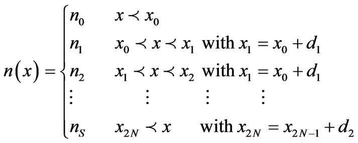
In order to study the electromagnetic waves propagating through photonic crystal structures and determine the optical properties of these periodic structures. We will explain in brief a mathematical treatment with a simple one dimensional photonic crystal structure (1DPC) (see Figure 1) which is composed of two materials with thicknesses ( and
and ) and refractive indices (
 and
and ) respectively. The analysis of the incident electromagnetic radiation on this structure will be performed using the transfer matrix method (TMM).
We will produce TMM in the form of the dynamical and the propagating matrices which had been used to describe the wave interaction through each layer and the wave response at the interfaces between these layers [12]. Our analysis will be start considering that, the electro-

Figure 1. Schematic diagram of 1D-binary structure; the thicknesses of its constituent materials are denoted by d1 and d2, respectively, and the corresponding refractive indices are separately indicated by n0, n1, n2, and ns, where n0 is the index of the air and ns is the index of substrate layer.
magnetic waves are propagating through the multilayer structure along x-direction, as shown in Figure 1. The used periodic structure can be defined along this direction as:
 (1)
(1)
The electric field of a general plane-wave solution can be written as , where
  is the z-component of the wave vector;
 ,
,  is the angle of the incident ray in each layer and c is the speed of light then the electric field distribution
  can be written as:
 (2)
(2)
where  is the x-component of the wave vector,
 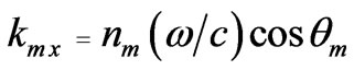 ,
,  and
and  represent the amplitudes of the plane wave at each interface
 . It’s wellknown that this distribution of the electric field was taken for
 , and we will now obtain the general case for N period. The amplitudes of the plane waves at different layers can be related by
 (3)
(3)
with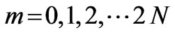 .
.
where matrices D (dynamical matrix) and P(propagation matrix) can be written as:
 (4a)
(4a)
 (4b)
(4b)
Since the propagation matrix can be written in the form of sine and cosine functions instead of the exponential function for simplifying
 (5)
(5)
where


The relation between the amplitudes of the plane wave can be written as
 (6)
(6)
where  is the matrix for one period without the effect of the vacuum and substrate, whose elements m11, m12, m21 and m22 was computed for TE-waves, which can be obtained also for TM-waves using the same analysis, and
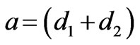 , is the lattice constant. This matrix can take the following form [12].
 (7)
(7)
with
 (8)
(8)
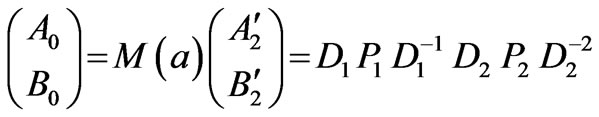
We can write the matrix of N periods in the form [12]:
 (9a)
(9a)
Since,
 (9b)
(9b)
where M(Na) is the matrix for N period, and Q11, Q12, Q21 and Q22 are parts of their elements that can be related to the elements of the single period matrix(m11, m12, m21, and m22) by the relations[13]:
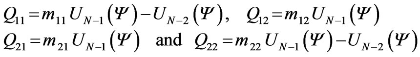 (10)
(10)
with
 (11)
(11)
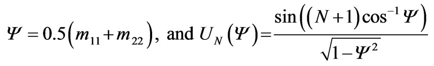
where , is Chebyshev polynomials of the second kind. Then by using the above expressions we can obtain the reflection and the transmission coefficients as:
 (12)
(12)
Finally we can calculate the transmittance and the reflectance using the following expressions:
 (13)
(13)
where
 (14)
(14)
This gives us the final form of the transmission and reflection coefficients for the incident electromagnetic waves inside this 1D-binary periodic structure as a function of the dynamical and the propagating matrices depending on the numerical solution of Maxwell’s using the TMM.
3. Results and Discussions
The periodicity of the permittivity plays the same role for the photons that propagate inside the structure than the atomic potential for the electrons. Leading further this analogy, the thicknesses and the index contrast of the photonic crystal determinate many of its optical properties as it does for conduction properties of semiconductors. We have used for our simulation Essential Macleod software. The Essential Macleod is a comprehensive software package for the design, analysis, manufacture and trouble shooting of thin film optical coatings. The program has a true multiple document interfaces. It can handle coatings from rugates to ultrafast, from singlelayer antireflection coatings to demanding color separation beamsplitters, providing all that is necessary for their design, analysis, production planning and even reverse engineering of a failed production attempt. A wide range of performance parameters, from straightforward transmittance and reflectance to color coordinates in different color spaces, is built into the software. It can synthesize designs from scratch or refine existing ones, investigate errors and extract optical constants of film materials for use in designs.
We can obtain the range of frequencies for which the kind of light cannot propagate inside the materials and the others can propagate. By reducing the size of the elementary cell of the periodic lattice, the frequencies can shift to higher values. The consequence of this property is the possibility to transpose a photonic crystal design from the microwave domain to infrared or visible range. In our results we have studied one dimensional metallic (different metals) dielectric (SiO2) photonic crystals (MDPC’s). For our calculations we have used the thickness of the dielectric (SiO2) layer is 344 nm, the thickness layer of metal is 5nm, the incidence of angle is 35˚ and the number of periods 10 for all our results.
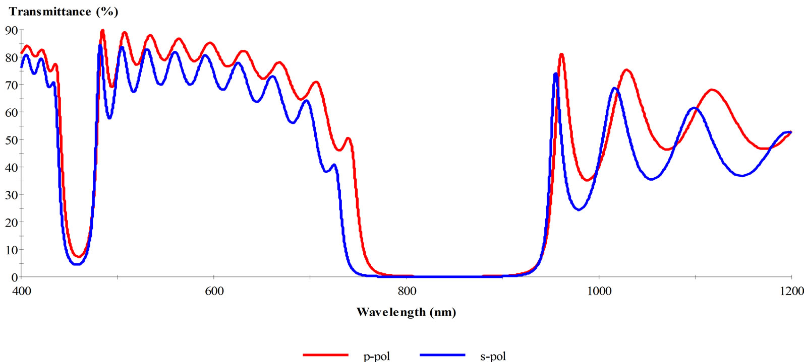
In the case of Ag-SiO2 (see Figure 2) we can see the magnitude of transmittance near the unity with visible light and there is a small photonic band gap (PBG) appeared within NIR (750 - 930 nm). The magnitude of transmittance in the case of Au-SiO2 (Figure 3) is less than 10% around 400 nm and increased to ~70 % within 550 - 700 nm and then we obtained the second and large PBG in the range 775 - 925 nm. In Figure 4, the magnitude of transmittance in the case of Cu-SiO2 is go downing around 60% within the range of visible light (400 - 700) and we obtained the same PBG between 775 - 925 nm.
In Figure 5, we have examined Al-SiO2 with the same conditions and we found Aluminum that gives the lowest possible transmittance within the visible and near IR frequencies with the complete PBG between 600 – 900 nm. The significance of the magnitude of incident angles also is obtained in Figure 6 with θ = 25˚, 30˚, 35˚ and 40˚. The behavior of incident angle has different influences on the forbidden bands of TE and TM modes. This work will be a useful reference when designing and producing some apparatus such as, optical filter, eyes-protecting to laser and heat-absorbing window.
4. Conclusions
We have studied metallic photonic crystals at visible and
 (a)
(a)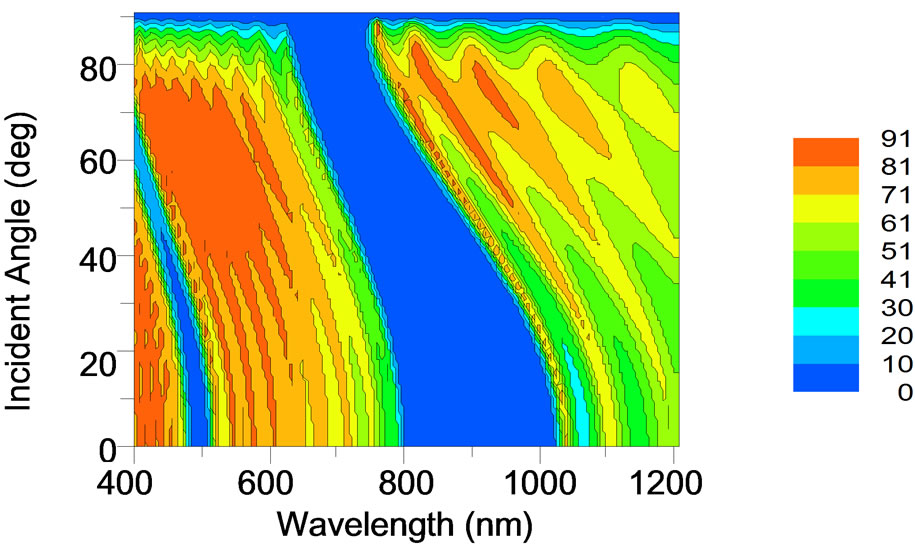 (b)
(b)
Figure 2. (a) The transmittance of p-pol, s-pol to Ag-SiO2 structure; (b) the incident angle dependence on wavelength to Ag-SiO2 structure.
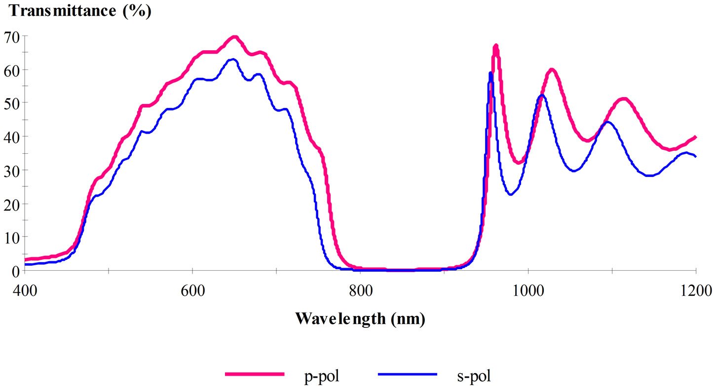
Figure 3. The transmittance of p-pol, s-pol to Au-SiO2 structure.
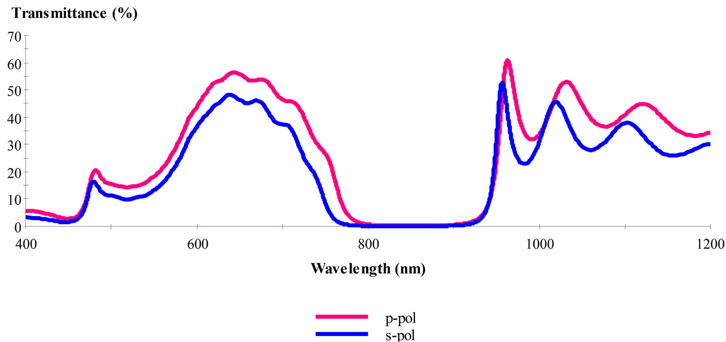
Figure 4. The transmittance of p-pol, s-pol to Cu-SiO2 structure.

Figure 5. The transmittance of p-pol, s-pol to Al-SiO2 structure.
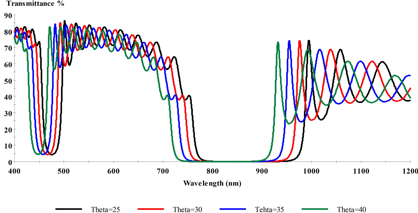
Figure 6. The significance of the incident angel’s θ = 25˚, 30˚, 35˚, 40˚ within Ag-SiO2 structure.
near-infrared wavelengths with the transfer matrix method. We focused on the transmittance of these structures, thus we studied the simple 1D structure. We expect that our conclusions regarding the transmittance will hold to any other metallic structures. By comparing the results for different metals, we found that copper gives the lowest possible transmittance within the visible frequencies. Silver gives slightly higher transmittance within the visible with small PBG near IR. Gold gives low possible transmittance within short visible and going to near 70% between 550 - 700 nm with small PBG within 750 - 850 nm. Aluminum is very lossy and is not recommended for optical photonic crystals. Silver and gold are acceptable although slightly lower in performance. We also found our results are very sensitive to the thickness of layers as well as PBG is sensitive to the kind of polarizations. This work will be a useful reference when designing and producing some apparatus such as, eyes-protecting to laser and heat-absorbing window.
5. Acknowledgements
The corresponding author Arafa H. Aly thankful Prof Macleod for his offers me the Essential Macleod program to achieve this work.
REFERENCES
- E. Yablonovitch, “Inhibited Spontaneous Emission in Solid-State Physics and Electronics,” Physical Review Letters, Vol. 58, No. 20, 1987, pp. 2059-2062. doi:10.1103/PhysRevLett.58.2059
- S. John, “Strong Localization of Photons in Certain Disordered Dielectric Superlattices,” Physical Review Letters, Vol. 58, No. 23, 1987, pp. 2486-2489. doi:10.1103/PhysRevLett.58.2486
- J. A. Sánchez-Gil and A. A. Maradudin, J. Q. Lu and V. D. Freilikher, “Transmission of Electromagnetic Waves through Thin Metal Films with Randomly Rough Surfaces,” Physical Review B, Vol. 51, No. 23, 1995, pp. 17100-17115. doi:10.1103/PhysRevB.51.17100
- M. M. Sigalas, C. T. Chan, K. M. Ho and C. M. Soukoulis, “Metallic Photonic Band-Gap Materials,” Physical Review B, Vol. 52, No. 16, 1995, pp. 11744-11751. doi:10.1103/PhysRevB.52.11744
- J. S. McCalmont, M. M. Sigalas, G. Tuttle, K. M. Ho and C. M. Soukoulis, “A Layer-by-Layer Metallic Photonic BandGap Structure,” Applied Physics Letters, Vol. 68, No. 5, 1996, pp. 2759-2761. doi:10.1063/1.115589
- A. H. Aly and S.-W. Ryu, “Study of Optical Transmission in Nanometallic Photonic Crystal,” Journal of Computational and Theoretical Nanoscience, Vol. 5, No. 4, 2008, pp. 597-601. doi:10.1166/jctn.2008.022
- D. Nau, A. Schönhardt, C. Bauer, A. Christ, T. Zentgraf, J. Kuhl and H. Giessen, “Disorder Issues in Metallic Photonic Crystals,” Physica Status Solidi (B), Vol. 243, No. 10, 2006, pp. 2331-2343. doi:10.1002/pssb.200668054
- A. H. Aly, “The Transmittance of Two Types of One-Dimensional Periodic Structures,” Materials Chemistry and Physics, Vol. 115, No. 1, 2009, pp. 391-394. doi:10.1016/j.matchemphys.2008.12.009
- A. H. Aly, S.-W. Ryu, H.-T. Hsu and C.-J. Wu, “THz Transmittance in One-Dimensional Superconducting Nanomaterial-Dielectric Superlattice,” Materials Chemistry and Physics, Vol. 113, No. 1, 2009, pp. 382-384. doi:10.1016/j.matchemphys.2008.07.123
- A. H. Aly, H.-T. Hsu, T.-J. Yang, C.-J. Wu and C.-K. Hwangbo, “Extraordinary Optical Properties of a Superconducting Periodic Multilayer in near-Zero-Permittivity Operation Range,” Journal of Applied Physics, Vol. 105, No. 8, 2009, pp. 083917-083923.
- J. D. Joannopoulos, S. G. Johnson, J. N. Winn and R. D. Meade, “Photonic Crystals Moleding the Flow of Light,” Princeton University Press, Princeton, 2008.
- P. Yeh, “Optical Waves in Layered Media,” John Wiley &Sons, New York, 1988.
- M. Born and E. Wofl, “Principles of Optics,” Cambridge, London, 1999.