Materials Sciences and Applications
Vol. 4 No. 5 (2013) , Article ID: 31463 , 6 pages DOI:10.4236/msa.2013.45036
Optical and Morphological Studies of Chemical Bath Deposited Nanocrystalline Cd1−xZnxS Thin Films
![]()
Department of Physics, Federal University of Technology, Minna, Nigeria.
Email: kasim309@futminna.edu.ng
Copyright © 2013 Kasim Uthman Isah. This is an open access article distributed under the Creative Commons Attribution License, which permits unrestricted use, distribution, and reproduction in any medium, provided the original work is properly cited.
Received March 13th, 2013; revised April 16th, 2013; accepted April 25th, 2013
Keywords: Chemical Bath Deposition; Cd1−xZnxS; Scanning Electron Microscope
ABSTRACT
Cadmium Zinc Sulfide, Cd1−xZnxS thin films were deposited by chemical bath deposition technique at bath temperature of 75˚C. The morphology of the films was analyzed by scanning electron microscope, the optical constants of the films were estimated from the transmission and reflection spectra of the films in the wavelength range of 300 - 900 nm. The films had a transmittance between 75% and 85% and optical band gap in the range 2.8 - 3.4 eV. The dependence of the refractive index of the films on the wavelength was investigated using the single oscillator model, from which the dispersion parameters were determined. The high frequency dielectric constant εL and the ratio of the carrier concentration to the effective mass N/m* were estimated based on the Spitzer and Fan model. Both εL and N/m* show a decrease in value with increase in Zinc content.
1. Introduction
Ultrathin semiconductor nanoparticle thin films have attracted growing interest for both fundamental research and technical application due to their size-dependent electronic properties that has lead to a wide range of technological applications as functional layers in electronic and optoelectronic devices, solar cells, photoelectrodes, photocatalysts, and sensors [1]. Nanocrystalline binary and ternary semiconductors of Groups II-VI have potential applications in many technical fields, including photoluminescence, solar cells and photovoltaic applications [2- 4].
CdS alloyed with ZnS form a continuous series of solid solution Cd1−xZnxS for the whole range of x, giving rise to a systematic variation of band gap of Cd1−xZnxS from 2.43 eV for CdS to 3.7 eV for ZnS. Besides, replacing CdS with the higher energy gap ternary Cd1−xZnxS has led to a decrease in window absorption loss, and has resulted in an increase in the short circuit current in thin film CdS window-based solar cells [5]. Also Cd1−xZnxS and related ternary compounds are promising materials for high density optical recording and for blue or even UV laser diodes applications based on the structure of Cd1−xZnxS which exhibit fundamental absorption edges that can vary from green to UV [6,7].
A number of film deposition methods such as chemical bath deposition (CBD), spray pyrolysis, vacuum evaporation, chemical vapor deposition, and sputtering have been used for preparing Cd1−xZnxS films [2,8-11].
In this work, the effect of Zn content on the optical properties and morphology of Cd1−xZnxS thin films deposited by chemical bath deposition technique are presented.
2. Experimental
Cd1−xZnxS thin films were deposited on Menzel-glazer glass slides. The chemicals used were cadmium acetate (Cd(CH3OO)2) of 0.015 M, zinc acetate (Zn(CH3COO)2) of 0.015 M and 0.05 M thiourea (SC(NH2)2). The concentration of ammonium acetate (NH4CH3COO) used as buffer was 0.3 M, while ammonia solution (NH3OH) concentration was 0.8 M. All chemicals were of analyticalgrade. A Bath temperature of 75˚C was used.
A 100 ml beaker was used as container for the reacting chemicals; this was immersed in a water bath. Solutions of cadmium acetate, zinc acetate, ammonium acetate and thiourea were first mixed together in the 100 ml beaker, heated to 75˚C and stirred vigorously.
Ammonia solution was then added and substrates immersed vertically. The concentrations and the amount of chemicals used are given in Table 1. The substrates had earlier been washed with detergent, rinsed in deionized water, soaked in nitric acid, degreased in ethyl alcohol and then rinsed in deionized water. The reacting bath was agitated throughout the period of deposition. The deposition was carried out for 45 minutes after which the coated substrates were removed and washed in de-ionized water to remove loosely adhered Cd1−xZnxS particles. The samples were labelled T1, T2 and T3 based on the three volumes of Zn(CH3COO)2 used.
The normal incidence optical transmittance of the films was measured in the scanning mode using the double beam α-Helios UV-Vis spectrophotometer, so modified to take a solid sample. The measurements were taken from a wavelength of 300 nm to 900 nm. The films morphologies were analyzed with a CARL ZEISS MA 10 scanning electron microscope (SEM).
3. Results and Discussion
3.1. Optical Properties and Dispersion Analysis
Specular yellow and adhesive Cd1−xZnxS films were obtained for the three films. The Transmittance spectra of the films are shown in Figure 1. The films had a transmittance of 78%, 75% and 85% in the visible region for the samples T1, T2 and T3 respectively.
The band gaps of the films were determined from electronic absorption spectra by the direct band gap method from the intercept of the plots of α2 versus energy hγ at α2 = 0, according to Tauc’s relation in the strong-absorption region of the films (Figure 2). The composition of the ternary Cd1−xZnxS was estimated from the expression given by the relationship [12],
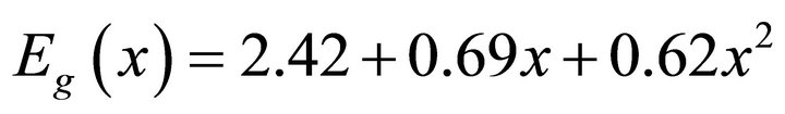
Eg(x) is the band gap of the composition of the ternary Cd1−xZnxS defined at x. The values of x determined from the expression are given in Table 2 for the three films. There is an increase in band gap with increase in Zn content x resulting from increase in the absorption edge.
The frequency dependent refractive index n of the thin films were determined from the equation [13],
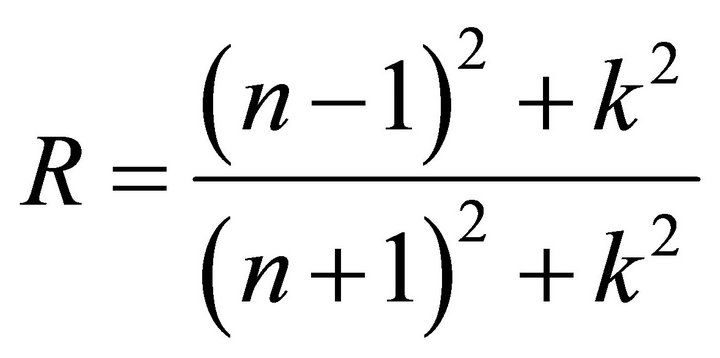

Figure 1. Transmittance spectra of the films.
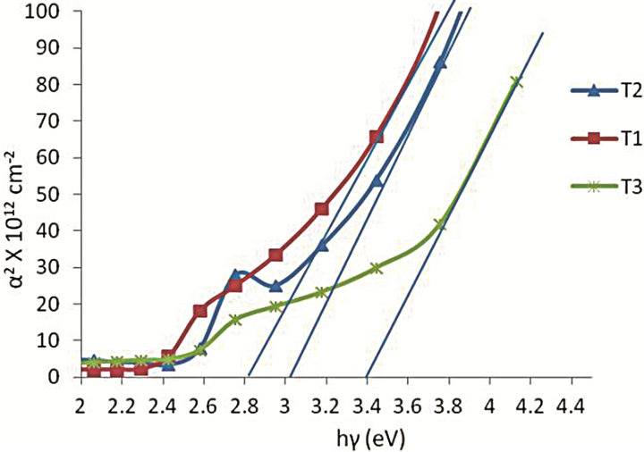
Figure 2. α2 versus hγ: Samples T1, T2 and T3.
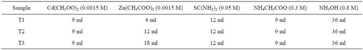
Table 1. Concentrations and volumes of chemicals used.
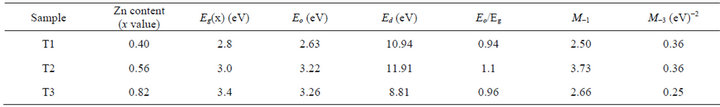
Table 2. Optical constants of the films.
where k 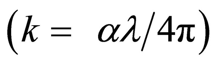 is the extinction coefficient. The spectral dependence of the refractive index n is shown in Figure 3. There is a sharp rise in n for the samples T1 and T2 at absorption edge towards the shorter wavelengths of the spectrum. This sharp onset of n at the absorption band edge is attributed to Van Hove singularity in the joint density of state in the excitation of transition between two bands [14].
The dispersion of the refractive index is related to the photon energy E (λ), by the single-oscillatory model proposed by Wemple and DiDomenico which describes the dielectric response for transitions below the interband absorption edge. Below the absorption edge, refractive index dispersion can be analyzed by the single-oscillator model [15]

where h is Planck’s constant, Eo is the average excitation energy for electronic transitions and is empirically related to the optical band gap, while Ed is the dispersion energy and is a measure of the average strength of interband optical transitions and can be considered as a parameter having very close relation with the charge distribution within unit cell and therefore with the chemical bonding [16]. The increase in Ed is associated with the evolution of the thin film microstructure to a more ordered phase [17]. The parameters Eo and Ed are obtained from the intercept and slope of the plot of (n2 − 1)−1 versus photon energy (hγ)2. Figure 4 shows an extended region of linearity of the plot, and is employed to determine these values. The obtained dispersion parameters change with deposition parameters.
Based on the single oscillator model, the single-oscillator parameters Eo and Ed are connected to the imaginary part εi of the complex dielectric constant and the −1
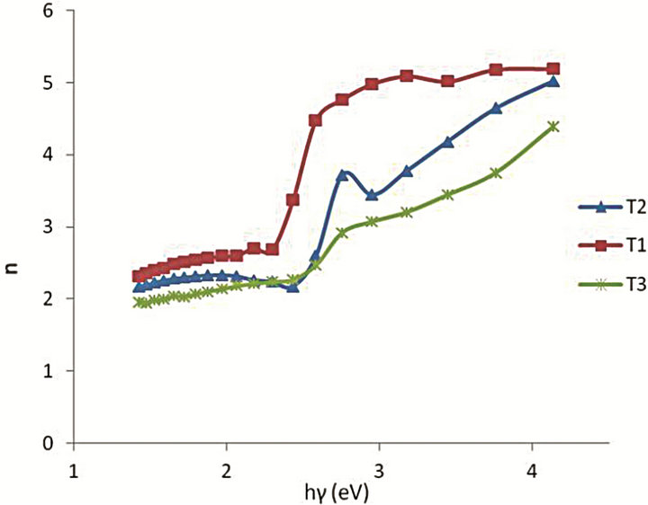
Figure 3. Variation of refractive index n with photon energy hγ of the films.
and −3 moments of the εi optical spectrum can be derived from the relations [18]:
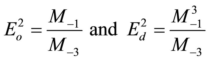
The determined values of M−1 and M−3 moments of the imaginary part εi of the dielectric constant of the samples as well the estimated values of the oscillator parameters and other values of the calculated optical parameters are summarized in Table 2.
The ratio Eo/Eg ≈ 1 is obtained for all the samples with a deviation of about ±0.1 eV. Ilican et al., had obtained a value of Eo/Eg ≈ 1.2 [19] in a similar work, using spray pyrolysis method in studying the influence of substrate temperature on the optical properties of CdZnS film. Sample T2 with x = 0.56 had the highest dispersion energy Ed of 11.91 eV, indicating it is of more ordered microstructure compared to samples T1 and T3.
It should be stressed that the oscillator energy E0 though very similar to the parameter used by Penn, being a measure of the energy difference between the “centers of gravity” of the valence and conduction bands [20], its value is different from the optical gap which probes the optical properties near the band edges of the material.
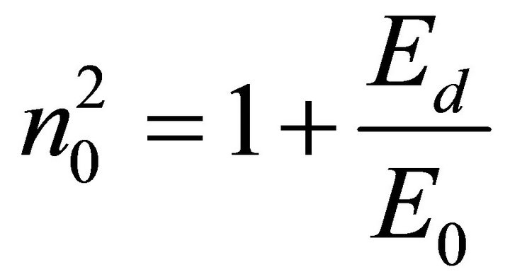
The refractive index at zero photon energy, also called the static refractive index no, given by the infinite wavelength dielectric constant 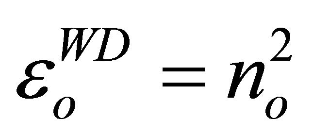 is determine from the dispersion relation [21]
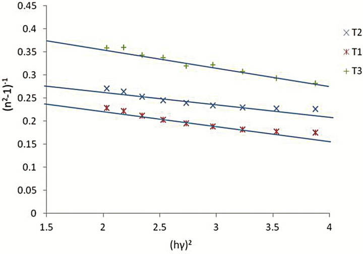
Figure 4. Plot of (n2 − 1)−1 versus photon energy (hγ)2 for Cd1−xZnxS thin films.
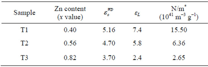
Table 3. Values of , εL and N/m*.
The values obtained for T1, T2 and T3 are 5.16, 4.70 and 3.70 respectively.
The high frequency dielectric constant is also given by [22]
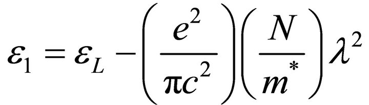
where ε1 is the real part of the dielectric constant, εL is the high frequency dielectric constant (or lattice dielectric constant) and N/m* is the ratio of carrier concentration to the effective mass. The real part of the dielectric constant ε1 = n2 was determined at different values of the wavelength λ in the transparent region. The plot of n2 against λ2 is given in Figure 5 and shows a linear dependence of n2 on λ2 in the transparent long wavelength region. Extrapolating the linear part of the plot to zero wavelength gives the value of εL and N/m* is determined from the slope. The values obtained are given in Table 3.
The difference between the values of  and εL obtained is attributed to the formation of free carriers in the thin films [23]. All the parameters in Table 2 tend to decrease with increase in Zn content.
3.2. Surface Morphology
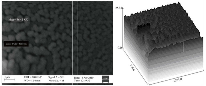
The SEM micrographs and the corresponding 3D topographical maps of the films are presented in Figures 6(a)- (c), they indicate that the surface morphology of the
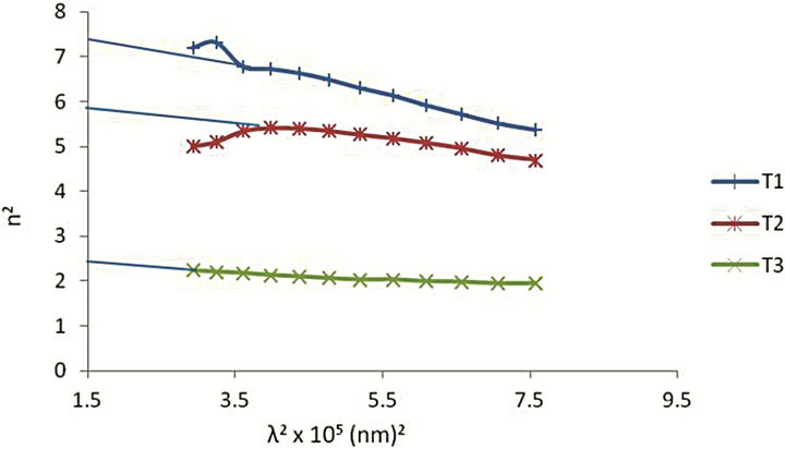
Figure 5. Plot of n2 versus λ2 for Cd1−x ZnxS thin films.
 (a)
(a)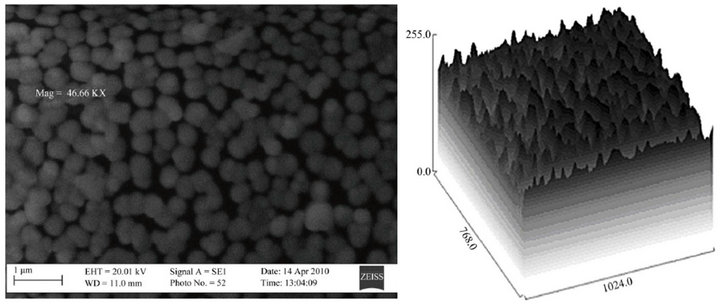 (b)
(b)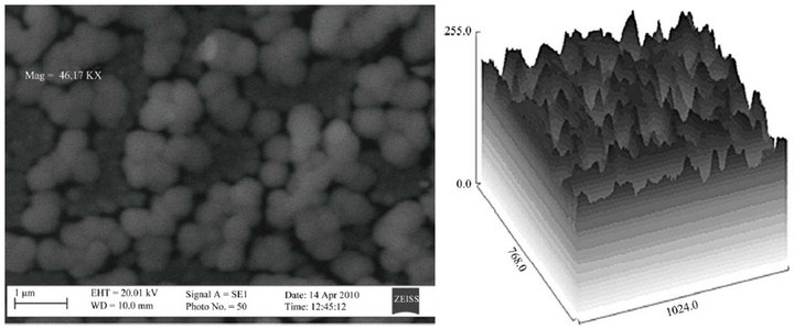 (c)
(c)
Figure 6. SEM micrograph of the films for samples (a) T1, (b) T2 and (c) T3.
films are influenced by the Zn content. The films show smooth and uniform spherical grains. The microstructure of the films are denser and more uniformly distributed for samples T1 and T2. The surface grain sizes were determined by the image analysis of several (ten) grains and the average values are 25, 11 and 13 nm for Samples T1, T2 and T3 respectively.
4. Conclusion
The effects of Zn content on optical and morphologicalproperties of Cd1−xZnxS thin film deposited by Chemical Bath Deposition technique been investigated. The optical band gaps Eg of the films were found to be between 2.8 and 3.4 eV. The average excitation energy for electronic transitions Eo, the dispersion energy Ed and the M−1 and M−3 moments of the εi were determined based on the single-oscillator model. The ratio Eo/Eg ≈ 1 for all the films. The sample with Zn content x = 0.56 showed a more ordered microstructure with the highest dispersion energy Ed of 11.9 eV. The high frequency dielectric constant εL and N/m* of all the samples were observed to decrease with increase in Zn content x.
REFERENCES
- N. I. Kovtyukhova, E. V. Buzaneva, C .C. Waraksa and T. E. Mallouk, “Ultrathin Nanoparticle ZnS and ZnS: Mn films: Surface Sol-Gel Synthesis, Morphology, Photophysical Properties,” Materials Science and Engineering B, Vol. 69-70, 2000, pp. 411-417. HUdoi:10.1016/S0921-5107(99)00312-8U
- J. Aguilar-Hernandez, J. Sastre-Hernandez, N. XimelloQuiebras, R. Mendoza-Perez, O. Vigil-Galan, G. ContrerasPuente and M. Cardenas-Garcia, “Photoluminescence Studies on CdS-CBD Films Grown by Using Different S/Cd ratios,” Thin Solid Films, Vol. 511-512, 2006, pp. 143- 146. HUdoi:10.1016/j.tsf.2005.11.082U
- D. Zubia, C. Lopez, M. Rodriguez, A. Escobedo, S. Oyer, L. Romo, S. Rogers, S. Quinonez and J. McClure, “Ordered CdTe/CdS Arrays for High-Performance Solar Cells,” Journal of Electrochemical Materials, Vol. 36, No. 12, 2007, pp. 1599-1603. HUdoi:10.1007/s11664-007-0276-4U
- T. Chandra and S. Bhushan, “Photoconducting and Photovoltaic Studies on Some Chemically Deposited (Cd-Zn)S & (Cd-Pb)S Films,” Journal of Materials Science, Vol. 39, No. 20, 2004, pp. 6303-6309. HUdoi:10.1023/B:JMSC.0000043600.30625.d1U
- T. D. Dzhafarov, F. Ongul and I. Karabay, “Formation of CdZnS Thin Films by Zn Diffusion,” Journal of Physics D, Appl Phys, Vol. 39, No. 15, 2006, pp. 3221. HUdoi:10.1088/0022-3727/39/15/001U
- W. Wang, I. Germanenko and M. Samy El-Shall, “RoomTemperature Synthesis and Characterization of Nanocrystalline CdS, ZnS, and CdxZn1−xS,” Chemistry of Materials, Vol. 14, No. 7, 2002, pp. 3028-3033. HUdoi:10.1021/cm020040xU
- T. Prem Kumar and K. Sankaranarayanan, “Growth and Characterization of CdZnS Thin Films by Short Duration Micro Wave Assisted-Chemical Bath Deposition Technique,” Chalcogenide Letters, Vol. 6, No. 10, 2009, pp. 555-562.
- S. Ilican, M. Caglar and Y. Caglar, “The Effect of Deposition Parameters on the Physical Properties of CdxZn1−xS Films Deposited by Spray Pyrolysis Method,” Journal of Optoelectronics and Advanced Materials, Vol. 9, No. 5, 2007, pp. 1414-1417.
- J. Lee, W. Songa, J. Yia, K. Yang, W. Han and J. Hwang, “Growth and Properties of the CdxZn1−xS Thin Films for Solar Cell Applications,” Thin Solid Films, Vol. 431-432, 2003, pp. 349-353. HUdoi:10.1016/S0040-6090(03)00526-1U
- P. B. Smith, “Low Temperature, Low Pressure CdZnS Films Produced by Metalorganic Chemical Vapor Deposition,” Journal of Vacuum Science and Technology, Vol. 10, No. 4, 1992, pp. 897-902. HUdoi:10.1116/1.577691U
- P. K. Ghosh, U. N. Maiti, S. F. Ahmed and K. K. Chattopadhyay, “Highly Conducting Transparent Nanocrystalline CdxZn1−xS Thin Film Synthesized by RF Magnetron Sputtering and Studies on Its Optical, Electrical and Field Emission Properties,” Solar Energy Materials & Solar Cells, Vol. 90, No. 16, 2006, pp. 2616-2629. HUdoi:10.1016/j.solmat.2006.02.015U
- D. S. Boyle, O. Robbe, D. P. Halliday, M. R. Heinrich, A. Bayer, P. O’Brien, D. J. Otway and M. D. G. Potter, “A Novel Method for the Synthesis of the Ternary Thin Film Semiconductor Cadmium Zinc Sulfide from Acidic Chemical Baths,” Journal of Materials Chemistry, Vol. 10, 2000, pp. 2439-2441. HUdoi:10.1039/b005544lU
- A. Abu EL-Fadl, G. A. Mohamad, A. B. Abd El-Moiz and M. Rashad, “Optical Constants of Zn1−xLixO Films Prepared by Chemical Bath Deposition Technique,” Physica B, Vol. 366, No. 1-4, 2005, pp. 44-54. HUdoi:10.1016/j.physb.2005.05.019U
- G. F. Bassani and G. P. Parravicini, “Electronic States and Optical Transitions in Solids,” Pergamon Press, Oxford, 1989.
- M. DiDomenico and S. H. Wemple, “Oxygen-Octahedra Ferroelectrics, I. Theory of Electro-Optical Effects,” Journal of Applied Physics, Vol. 40, No. 2, 1969, pp. 720-735. HUdoi:10.1063/1.1657458U
- H. S. Afak, M. Merdan and O. F. Yüksel, “Dispersion Ana- lysis of SnS and SnSe,” Turkish Journal of Physics, Vol. 26, No. 5, 2002, pp. 341- 347.
- S. H. Wemple, “Refractive-Index Behaviour of Amorphous Semiconductors and Glasses,” Physics Review B, Vol. 7, No. 8, 1973, pp. 3767-3777. HUdoi:10.1103/PhysRevB.7.3767U
- A. M. Salem, “Structure, Refractive-Index Dispersion and the Optical Absorption Edge of Chemically Deposited ZnxCd1−xS Thin Films,” Applied Physics A, Vol. 74, No. 2, 2002, pp. 205-211. HUdoi:10.1007/s003390100877U
- S. Ilican, Y. Caglar and M. Caglar, “Effect of the Substrate Temperatures on the Optical Properties of the Cd0.22Zn0.78S Thin Films by Spray Pyrolysis Method,” Physica Macedonica, Vol. 56, 2006, pp. 43-48.
- S. H. Wemple and M. Di Domenico Jr., “Optical DisperSion and Structure of Solids,” Physics Review Letters, Vol. 23, No. 20, 1969, pp. 1156-1160. HUdoi:10.1103/PhysRevLett.23.1156U
- O. A. Azim, M. M. Abdel-Aziz and I. S. Yahia, “Structure and Optical Analysis of Ta2O5 Deposited on Infrasil Substrate,” Applied Surface Science, Vol. 255, No. 9, 2009, pp. 4829-4835. HUdoi:10.1016/j.apsusc.2008.11.084U
- W. G. Spitzer and H. Y. Fan, “Determination of Optical Constants and Carrier Effective Mass of Semiconductors,” Physical Review, Vol. 106, No. 5, 1957, pp. 882- 890. HUdoi:10.1103/PhysRev.106.882U
- M. M. El-Nahass, A. A. M. Farag, E. M. Ibrahim and S. Abd-El-Rahman, “Structural, Optical and Electrical Properties of Thermally Evaporated Ag2S Thin Films,” Vacuum, Vol. 72, No. 4, 2004, pp. 453-460. HUdoi:10.1016/j.vacuum.2003.10.005U