Circuits and Systems
Vol.06 No.01(2015), Article ID:53422,6 pages
10.4236/cs.2015.61002
A Static Phase Offset Reduction Technique for Multiplying Delay-Locked Loop
Xinjie Wang, Tadeusz Kwasniewski
Department of Electronics, Carleton University, Ottawa, Canada
Email: xiwang@doe.carleton.ca, tak@doe.carleton.ca
Copyright © 2015 by authors and Scientific Research Publishing Inc.
This work is licensed under the Creative Commons Attribution International License (CC BY).
http://creativecommons.org/licenses/by/4.0/


Received 28 December 2014; accepted 18 January 2015; published 21 January 2015
ABSTRACT
Static phase offset (SPO) in conventional multiplying delay-locked loops (MDLLs) dramatically degrades the deterministic jitter performance. To overcome the issue, this paper presents a new SPO reduction technique for MDLLs. The technique is based on the observation that the SPO of MDLL is mainly caused by the non-idealities on charge pump (e.g. sink and source current mismatch), and control line (e.g. gate leakage of loop filter and voltage controlled delay line (VCDL) control circuit). With a high gain stage inserting between phase detector/phase frequency detector (PD/PFD) and charge pump, the equivalent SPO has been decreased by a factor equal to the gain of the gain stage. The effectiveness of the proposed technique is validated by a Simulink model of MDLL. The equivalent SPO is measured by the power level of reference spur.
Keywords:
Static Phase Offset, Multiplying Delay-Locked Loop, Deterministic Jitter, Reference Spur, PLL

1. Introduction
In high-speed data communication systems, on-chip clock multiplication plays a very important role. Phase- locked loops (PLLs) and multiplying delay locked loops (MDLLs) are widely employed to generate the accurate high-frequency on-chip timing signals from a low frequency, low jitter clock source. If a ring voltage controlled oscillator (VCO) is used in a PLL, the effect of accumulation of oscillator noise will be significant. VCO noise is mainly induced by the noise of power supply, substrate and the control line. Although a high-quality LC-tank oscillator can significantly reduce the effect of noise accumulation, it has a relatively small tuning range and occupies a large die area. This makes LC-tank VCO not the best candidate for data recovery and difficult to integrate. But an MDLL does not accumulate the noise over many cycles on VCDL. Most of the MDLLs are first-order systems; this means that it does not rely on a wide loop-bandwidth to correct for VCDL jitter; consequently the jitter peaking is negligible [1] and the system is also unconditionally stable.
However, relatively high reference spur caused by SPO between the reference edge and its counterpart of MDLL output dramatically degrades its deterministic jitter performance. Different techniques of reducing SPO in MDLL have been reported [2] -[7] .
[2] proposed a method to inject the clean reference edges with different phases into different delay stage of VCDL pseudo-randomly. So the SPO also pseudo-randomly showed up on different MDLL output cycle in one reference period. Theoretically the reference spur can be lowered by 20log(N) dB, where N is the division ratio. In [3] a narrow bandwidth auxiliary loop is employed to compensate for the mismatch of charge pump current. Similar to [3] , a digital method has been proposed in [4] . In [5] the MDLL output signal is firstly divided by 2, then the divided two parts are sampled by a high-resolution time to digital converter (TDC) separately and finally the results are compared to generate phase error control signal. Similar to [5] , a 1-bit TDC and a low- bandwidth delay-tuning path has been employed. The low-bandwidth ensures to supress the TDC quantization noise to be low enough. In [6] , the design focused on positioning of control signal of MUX which selected the clean reference edge or the delay line output feedback signal and the design also focused on a highly matched charge pump (CP). [7] proposed a fractional-N MDLL. A digital to time (DTC) block has been proposed to generate fine-resolution varying reference edge to compensate for SPO.
Although the reference spur performance of MDLL has been improved with all the reported SPO reduction techniques, it still cannot compare with that of PLL. Research effort is still largely needed. To attempt to shorten the research gap, this work proposed a new SPO reduction technique that is inserting a gain stage between PD/PFD and charge pump to achieve lower equivalent SPO.
2. Background
2.1. Operation Principle of MDLL
Typically, MDLL can be divided into two types, edge combiner based and cyclic reference injection based. For the edge combiner based MDLL shown in Figure 1(a), the frequency multiplication is realized by combining the reference edges propagating in the VCDL with equally spaced phases. Compared with the PLL based clock generator, this implementation is easier to design but multiplication ratio is fixed and the mismatches in the delay stages and edge-combining logic significantly contribute the output deterministic timing jitter.
The cyclic reference injection based MDLL shown in Figure 1(b) is very similar as a PLL except for the extra MUX and Select Logic blocks. With the MUX, the VCDL output is fed back to its input, and forms a ring VCO as MUX control signal Sel is 0. When Sel changes to 1, the rising edge of reference signal fref will inject and propagate in the VCDL. And the clean reference edge resets the phase noise accumulated in the previous M-1 cycles. The high-frequency signal generated from the VCO-like VCDL is divided by the divider and a pulse signal last is generated at every M cycles. The last signal triggers the select logic to generate Sel. The signal Sel also enables the phase detector to produce the phase difference between the rising edge of fref and its counterpart of fout then feed it to charge pump to generate the VCDL control signal Vctrl to adjust the delay of VCO-like VCDL. This type of MDLL can easily achieve frequency programmable multiplication. Another significant advantage over the edge combiner based MDLL is that the output frequency is less sensitive to the mismatch among the VCDL. Because each edge of the output passes through the same delay element, the fixed pattern jitter due to mismatch among delay stages is avoided.
2.2. Mechanisms of SPO
In PLL, SPO does not cause as much reference spur as MDLL does because in PLL the reference edge does not replace the counterpart of VCO output. SPO in PLL and MDLL is shown in Figure 2. It can be seen that although PLL output has SPO, the period of the Nth cycle is almost the same as the average period of other cycles. However, comparing with PLL output, if MDLL output has SPO, the period of Nth cycle is much different (either larger or smaller) from the average period of other cycles. SPO is mainly caused by the sink and source current mismatch in charge pump and the current leakage on the control line. The charge pump output current in locked state due to mismatch is shown in Figure 3. Please refer to [8] for more detailed analysis about charge pump current mismatch.
The SPO can be calculated in both phase and time domain [8] [9] . In the case with leakage current on control line,
 (a) (b)
Figure 1. (a) Edge combiner based MDLL; (b) Cyclic reference injection based MDLL.

Figure 2. PLL/MDLL output signal in locked state; (a) PLL/MDLL reference signal; (b) PLL output with positive SPO; (c) PLL output with negative SPO; (d) MDLL output with positive SPO; (e) MDLL output with negative SPO.

Figure 3. Charge pump output current in locked state due to mismatch [10] .
 (1)
(1)
where ϕSPO and τ are the phase and time domain static phase offset, Tref is the period of reference signal, Ileak is the leakage current on control line and ICP is the average charge pump current. In the case of sink and source current mismatch in charge pump,
 (2)
(2)
where Treset is the reset time of tri-state phase frequency detector (PFD), IUP and IDN are the source and sink current of charge pump. Here IUP is assumed to be larger than IDN. If IDN is larger than IUP, Equation (2) can be expressed as
 (3)
(3)
3. Proposed SPO Reduced MDLL
3.1. Concept of the Proposed SPO Reduction Technique
The concept of block diagram of the proposed SPO reduction technique is shown in Figure 4. Figure 4(a) shows the S-domain model of cyclic reference injection based MDLL. To model the edge combiner based MDLL, the only requirement is to change the division ratio to “1” because the loop (shown in Figure 1(a)) essentially is a DLL. The SPO shown in Figure 2(c)-(d) is modeled as phase error Δθ shown in Figure 4(b). Because the charge pump current mismatch and leakage current on the control line are not proportional to charge pump current value, if a high gain stage with gain of G is inserted between PD/PFD and charge pump shown in Figure 4(c), at the same time decrease the charge pump current by a factor of G, the loop characteristic is not changed but the equivalent SPO has been decreased to Δθ/G shown in Figure 4(d).
3.2. Proposed SPO Reduced MDLL
To achieve a gain stage between the PD/PFD and charge pump, one possible way is to employ time amplifiers to amplify the UP and DN pulses width of tri-state PFD. Another way is to convert the time domain signal, VCDL output phase signal, to a voltage signal. Because to process a voltage-domain signal is much easier than to process a time-domain signal this work adopted the second method. Figure 5(a) shows the proposed MDLL. Comparing with the conventional one shown in Figure 1(b), the PD of this MDLL shown in Figure 5(b) has only one input which is the output of VCDL. The architecture can dramatically reduce the error caused by path mismatch due to avoiding comparison of two different edge signals as conventional PFD does. The PD consists of a period to voltage converter and a delta modulator. As shown in Figure 4(c)-(d), the first N-1 cycles of MDLL output waveforms have evenly distributed in-lock error and the Nth cycle has either larger or smaller period. The operation principle of PD is: firstly the VCDL output fout is converted to a voltage signal based on each period through a period to voltage converter then the converted voltage signal of Nth cycle is sampled by Sel1 to produce Vinst. The converted voltage signal of the first N-1 cycles is sampled by Sel2 and goes into a delta modulator to generate the period average signal Vave. The simplified timing diagram of PD is shown in Figure 6. The delta modulator provides a highly accurate average period of the first N-1 cycles of VCDL output. Vinst subtracts Vave through V/I circuit shown in Figure 5(c) to extract SPO information and this information is converted to the VCDL control voltage Vc.
4. Simulation Results
The proposed MDLL described above was verified by a behavioral model built in Simulink shown in Figure 7. It mainly consists of a VCDL modeled with a Variable Delay Line, a divider with division ratio of 10, a block of Extract period value extracting each cycle period value from VCDL output fout waveform and a block of PD + V/I shown in Figure 8 extracting SPO. Loop filter capacitor is modeled with Integrator1. Loop Gain1 is the product of factor of period to voltage conversion, factor of voltage to current conversion, loop filter gain and VCDL gain. Tn in Figure 8 is the n-th output period, G1 is the gain of period to voltage converter equivalent to the gain of the gain stage in Figure 4. (G1*G2) is equivalent to the gain of the integrator in Figure 5(b). The Nth period is deducted by the integrated value to extract the period error value which is integrated again to generate a new average period value. This procedure will be repeated as long as the circuit operates. Since the main in-lock error appears in the last period within one reference cycle, this error detection is controlled by Sel1. Then the error value is sent to loop filter to generate a control voltage to tune the VCDL delay. Non-idealities caused SPO is modeled as an additive constant which is labeled as “SPO” shown in Figure 8. This “SPO” has the unit of time.
The reference signal fref is 100MHz, division ratio is 10 and the Initial propagation delay is 480 ps. Loop Gain1 = 1.28 e4 and TranSPOrt Delay2 = 2.5 ns. Simulation results of the MDLL output signal spectra are shown in Figure 9. The center frequencies in all of the spectra plots are 1 GHz. In Figure 9(a), the SPO and G1 are set to 0 and 1 respectively, the spectrum plot shows that the reference spur has similar power to noise floor. In Figure 9(b),
 (a)
(a) (b)
(b) (c)
(c) (d)
(d)
Figure 4. Concept of block diagram of the proposed SPO reduction technique; (a) S-domain model of MDLL; (b) S-domain model of MDLL with SPO Δθ; (c) S-do- main model of MDLL with SPO Δθ; and a gain stage insertion; (d) Equivalent SPO becoming Δθ/G after a gain stage insertion.
 (a)
(a)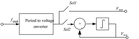 (b)
(b)
Figure 5. (a) Block diagram of proposed MDLL; (b) Block diagram of PD; (c) Schematic of V/I.

Figure 6. Simplified timing diagram of PD.

Figure 7. Simulink model of proposed MDLL.

Figure 8. Model of PD + V/I.

 (a) (b)
 (c) (d)
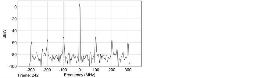
Figure 9. Spectral plots of VCDL output under different conditions (a) SPO = 0, G1 = 1; (b) SPO = 2e−12, G1 = 1; (c) SPO = 2e−12, G1 = 10; (d) SPO = 2e−12, G1 = 50.
SPO = 2e−12 and G1 = 1, the reference spur is about −30 dBc. In Figure 9(c), SPO = 2e−12 and G1 = 10, the reference spur is about −50 dBc. In Figure 9(d), SPO = 2e−12 and G1=50, the reference spur is about −64 dBc.
5. Conclusion
A concept of static phase offset reduction technique for MDLL has been proposed. The concept is also effective for PLL. A SPO reduction MDLL based on the concept has been proposed. It is verified by a behavioral simulink model. The simulation results validated both the proposed concept and the SPO reduction MDLL. The reduced equivalent SPO is measured by the power of reference spur level.
Acknowledgements
The authors are thankful to the reviewers for their insightful queries, constructive criticisms and helpful suggestions, which improved the presentation of the paper considerably.
References
- Farjad-Rad, R., Dally, W., Ng, H.-T., Senthinathan, R., Lee, M.-J.E., Rathi, R. and Poulton, J. (2002) A Low-Power Multiplying DLL for Low-Jitter Multigigaherz Clock Generation. IEEE Journal of Solid State Circuit, 37, 1804-1811. http://dx.doi.org/10.1109/JSSC.2002.804340
- Liu, C.-Y. and Chen, W.-Z. (2011) Spur Suppression Technique for Multiplied Delay Locked Loop. Proceedings of IEEE International Symposium on Radio Frequency Integration Technology (RFIT), 153-156.
- Du, Q.J., Zhuang, J.C. and Kwasniewski, T. (2006) A Low-Phase Noise, Anti-Harmonic Programmable DLL Frequency Multiplier with Period Error Compensation for Spur Reduction. IEEE Transactions on Circuits Systems II, 53, 1205-1209. http://dx.doi.org/10.1109/TCSII.2006.883103
- Elshazly, A., Inti, R., Young, B. and Hanumolu, P.K. (2013) Clock Multiplication Techniques Using Digital Multiplying Delay-Locked Loops. IEEE Journal of Solid-State Circuits, 48, 1416-1428. http://dx.doi.org/10.1109/JSSC.2013.2254552
- Helal, B.M.M., Straayer, Z., Wei, G.-Y. and Perrott, M.H. (2008) A Highly Digital MDLL-Based Frequency Multiplier That Leverages a Self-Scrambling Time-to-Digital Converter to Achieve Subpicosecond Jitter Performance. IEEE Journal of Solid-State Circuits, 43, 855-863. http://dx.doi.org/10.1109/JSSC.2008.917372
- Ali, T.A., Hafez, A.A., Drost, R., Ho, R. and Yang, C.-K.K. (2011) A 4.6 GHz MDLL with −46 dBc Reference Spur and Aperture Position Tuning. ISSCC, Dig. Tech. Papers, 466-468.
- Marzin, G., Levantino, S., Samori, C. and Lacaita, A.L. (2014) A 1.7 GHz MDLL-Based Fractional-N Frequency Synthesizer with 1.4 ps RMS Integrated Jitter and 3 mW Power Using a 1b TDC. ISSCC, Dig. Tech. Papers, 360-362.
- Rhee, W. (1999) Design of High Performance CMOS Charge Pumps in Phase Locked Loop. Proceedings of IEEE International Symposium on Circuits and Systems (ISCAS), 1, 545-548.
- Fischette, D. (2009) First Time, Every Time Practical Tips for Phase Locked Loop Design. http://www.delroy.com/PLL_dir/tutorial/PLL_tutorial_slides.pdf
- Shu, K. and Sanchez-Sinencio, E. (2005) CMOS PLL Synthesizers: Analysis and Design. Springer, Berlin.