Journal of Applied Mathematics and Physics
Vol.05 No.05(2017), Article ID:76502,7 pages
10.4236/jamp.2017.55097
Normalized Area Solar Cell and Potential Applications
Marcel Pasquinelli, Jean-Jacques Simon, Judikael Le Rouzo, François Flory, Ludovic Escoubas
Aix Marseille Université, CNRS, Université de Toulon, IM2NP UMR 7334, Marseille, France

Copyright © 2017 by authors and Scientific Research Publishing Inc.
This work is licensed under the Creative Commons Attribution International License (CC BY 4.0).
http://creativecommons.org/licenses/by/4.0/


Received: April 10, 2017; Accepted: May 22, 2017; Published: May 26, 2017
ABSTRACT
Nowadays in laboratories and in industries, distribution of solar cells sizes could be very large, hence; for the first time it is rather difficult to compare photovoltaic parameters which are size dependent (current, serial resistance, shunt resistance...) and performances of these cells. Also, it will be useful for scale effect to extrapolate performances calculated on a unit size solar cell to commercial products, especially in the case of heterogeneous wafers used for the device.
Keywords:
Photovoltaic, Solar Cell, Efficiency, Serial Resistance, Shunt Resistance

1. Introduction
In this work, we have focused our model on standard multicrystalline p-type silicon solar cells; the standard solar cell was produced by the most industries in 2011. Because of better radiations hardness and the primary spatial domain applications, p-type bulk silicon is the first studied and produced solar cell [1] .
2. Methodology
We have both used PC1D [2] software and experimental measurement on commercial solar cells in order to extract parameters for our electrical model used with SPICE software [3] (Figure 1).
Single diode model for illuminated solar cell could be used here [4] [5] [6] , this model takes in account the shunt across the junction (rsh), the lumped resistance (rs).
In this model, the output (I-V) characteristic is given by the Equation (1)

Figure 1. One diode electrical model of illuminated solar cell.
(1)
Equation (1): (I-V) analytical expression for one exponential model solar cell
The difficulty in equation 1is that two kinds of parameters coexists, intensive parameter such as voltage (V), temperature (T),… and extensive ones such as current (I), resistances (Rs and Rsh). If we want a quantitative comparison between solar cells with different surface areas (S), it is necessary to give the current density, J, versus voltage, V, equation. This expression is simply derived from (1) with the assumption:
(2)
(3)
We can now introduce a normalized area solar cell (S = 1 cm2 for instance) with resistance specifications given in Ω∙cm2 units.
(4)
and
(5)
(6)
It is now obvious that for a given solar cell (material and process) the serial and shunt resistance decrease if the area increases. To highlight this, for two solar cells with S and S' area respectively and if S' > S, Equations (4)-(6) imply that:
(7)
and
(8)
For instance, if ,
(9)
and
(10)
Best values for parameters used in Equation (6)
To estimate Jo, Jph, a, rs and rsh values, we have made some statistical measurements on elaborated solar cells characterized under standard one sun test condition (AM1, 5G) (Table 1).
3. Applications and Results
3.1. Surface Area Effect on Photovoltaic Properties in One Sun Application
Thanks to this model, it is relatively easy to extrapolate photovoltaic parameters computed for a unit size solar cell to another size, just by calculating Rs and Rsh for the size S. The formula used in this case is:
For size S:
(11)
and
(12)
In order to verify this assumption, PC1D and SPICE codes are used, we have modelized a unit solar cell with parameters generally used in conventional p- type silicon solar cells. Table 2 shows values obtained for three surface areas, it is clear that these results are in good agreement with the previous assumption.
3.2. Serial Resistance Loss in Concentrated Photo Voltaic CPV Solar Cells
Concentrated photovoltaic is very attractive due to the fact that for the same solar cell size, the photovoltaic properties are increased with X, when the device is illuminated under X sun.
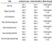
Table 1. Electrical and photovoltaic parameters average values for p-type multi-crystal- line silicon solar cells (surface area size = 1 cm2).
Table 2. Evolution of photovoltaic parameters with the surface areas of the cells.
A current question is whether conventional solar cells can be used for low concentration applications, typically X < 10.
With our model, it is evident that it is not possible, because of the high serial resistance value.
In fact, Figure 2(a) and Figure 2(b) show the drastic effect of the serial resistance. If solar flux is concentrated on conventional solar cells (rs = 1.5 Ω∙cm2), Jsc increases linearly if X < 10 and saturates after this value, but and most importantly, there is a decrease in conversion efficiency.
If you want to optimise this possible utilisation for conventional solar cells, the rs value must be divided by a factor of ten (rs = 0.15 Ω∙cm2), which is not easy with today’s technology.
 (a)
(a) (b)
(b)
Figure 2. (a) Short circuit current density evolution with concentration factor for two serial resistances values. (rs = 1.5 Ω∙cm2 and 0.15 Ω∙cm2); (b) conversion efficiency evolution with concentration factor for two serial resistances values.
3.3. Solar Cell Modelized by N Unit Solar Cells (U.S.C)
In a solar cell, global performances are largely relative to local ones, specifically in heterogeneous material such as multi-crystalline silicon.
To evaluate local properties it is useful to divide a large size into N unit solar cells, in Figure 3 in order to illustrate this method, we have chosen N = 4, the U.S.Cs are connected in parallel.
Application 1: Homogeneous solar cell
For this case each unit solar cells are identical (Figure 4).
Evidently, the performances for the final solar cell are conserved, but this ideal case could be attributed to an homogeneous solar cell, in terms of materiel, for instance monocrystalline wafer and uniform processes.
Generally, especially for multicrystalline ingots, heterogeneous properties govern final solar cell performances. In a rapid approach we can evaluate the effects of local defects at the scale of individual USC on global performance, such as local shunt (rsh), local bad electrical contact (rs) and local bad photon collection or conversion (Jph)
Now, to evaluate the impact of unit solar cells on the final device, we have chosen to see the influence of rs, rsh and Jph after a 50% variation of their initial value.
Application 2: Serial resistance discrepancy
In the electrical model Figure 1, serial resistance rs is a lumped value that takes into account contact resistance on the emitter and the base, grid line con- tact and semiconductor resistivity. This final value depends greatly on the process and also on possible degradation during the solar cell's lifetime.

Figure 3. Homogeneous solar cell composed by four parallel unit solar cells.

Figure 4. Homogeneous solar cell parameters. (a): U.S.C parameters; (b) Solar cell made by four distributed homogeneous U.S.C: and (c) Final solar cell parameters.
In this case, illustrated by Figures 5(a)-(c), we have just increased the rs value for one cell, this modified value is equal to 2.25 ohms, which represents also 50% variation. We can see in Figure 5(c), that only conversion efficiency of the solar cell is affected and decreases to 14.81%.
Application 3: Shunt resistance discrepancy
For this case, we have taken into account a 50% decrease of the shunt resistance in the unit solar cell (Figures 6(a)-(c)). Especially in multicristalline wafers, shunt leakage must be attributed to crystallographic defects decorated with metallic impurities crossing the junction. During the solar cell fabrication, shunt resistance degradation must appear at the aperture of the junction process.
We can see that for this local variation, the total properties of the cell are not greatly affected, but evidently if the shunt leakage increases the impact will be more important.
Application 4: Local photocurrent generation discrepancy
This case must be attributed to an accidental partial shadowing of the cell, or more problematically to a local area with poor electronic quality due to the presence of electrical recombining impurities for instance.
We have also kept with the same total variation (50%) of the unit Jsc value, 17.5 mA/cm2 instead of 35 mA/cm2, and the results are described in Figures 7(a)-(c).
It is obvious that this situation is the worst case, because of the degradation of all photovoltaic parameters (Voc, Jsc and η).

Figure 5. Serial resistance discrepancy. (a) U.S.C parameters; (b) Solar cell made by four distributed U.S.C: and (c) Final solar cell parameters.

Figure 6. Shunt resistance discrepancy. (a) U.S.C parameters; (b) Solar cell made by four distributed U.S.C: and (c) Final solar cell parameters.

Figure 7. Local photocurrent generation/recombination discrepancy. (a) U.S.C parameters; (b) Solar cell made by four distributed U.S.C: and (c) Final solar cell parameters.
4. Conclusions
We have proposed a method seeking to explain properties of solar cell by local analysis thanks to a normalized area solar cell concept. We studied here the influence of three macroscopic parameters (rs, rsh and Jsc); these parameters depend at the same time on implemented materials and on the solar cell technology. A principal result is that the contribution of local photo-current density (Jsc) is the most important.
Most of actual solar cell technologies are based on multicrystalline materials (Si, CIGS, CdTe,) and for each category as we have done for silicon, parameters for each unit solar cell must be defined.
As we have described in this article, several applications could be concerned with this analysis and for further studies, it will be such interesting to implement and compare this model with local photoelectrical characterizations as Light Beam Induced Current (LBIC), Photoluminescence and Electroluminescence Imaging.
Cite this paper
Pasquinelli, M., Simon, J.-J., Le Rouzo, J., Flory, F. and Escoubas, L. (2017) Normalized Area Solar Cell and Potential Applications. Journal of Applied Mathematics and Physics, 5, 1106- 1112. https://doi.org/10.4236/jamp.2017.55097
References
- 1. Cotter, J.E., Guo, J.H., Cousins, P.J., Abbott, M.D., Chen, F.W. and Fisher, K.C. (2006) P-Type versus N-Type Silicon Wafers: Prospects for High-Efficiency Commercial Silicon Solar Cells. IEEE Transactions on Electron Devices, 53, 1893-1901. https://doi.org/10.1109/TED.2006.878026
- 2. Clugston, D.A. and Basore, P.A. (1997) PC1D Version 5: 32-Bit Solar Cell Modelling on Personal Computers. 26th IEEE Photovoltaic Specialists Conference, Anaheim, 30 Sepember-3 October 1997, 207-210.
- 3. Nageland, L.W. and Pederson, D.O. (1973) SPICE (Simulation Program with Integrated Circuit Emphasis). Memorandum No. ERL-M382, University of California, Berkeley.
- 4. Charles, J.P., Abdelkrim, M., Muoy, Y.H. and Mialhe, P. (1981) A Practical Method of Analysis of the Current-Voltage Characteristics of Solar Cells. Solar Cells, 4, 169-178.
- 5. Kaminsky, A., Marchand, J.J. and Laugier, A. (1999) I-V Methods to Extract Junction Parameters with Special Emphasis on Low Series Resistance. Solid State Electronics, 43, 741-745.
- 6. Chegaar, M., Ouennoughi, Z., Guechi, F. and Langueur, H. (2003) Determination of Solar Cells Parameters under Illuminated Conditions. Journal of Electron Devices, 2, 17-21.