Paper Menu >>
Journal Menu >>
 Wireless Sensor Network, 2010, 2, 18-30 doi:10.4236/wsn.2010.21003 anuary 2010 (http://www.SciRP.org/journal/wsn/). Copyright © 2010 SciRes. WSN Published Online J VLSI Implementation for Low Noise Power Efficiency Cellular Communication Systems Rondia MACK, Maher RIZKALLA, Paul SALAMA, Mohamed EL-SHARKAWY Department of Electrical and Computer Engineering, Indiana University Purdue University Indianapolis, Indianapolis, USA Email: {mrizkall, psalama}@iupui.edu Received October 24, 2009; revised November 16, 2009; accepted November 25, 2009 Abstract A low power model for Code Division Multiple Access (CDMA) based cellular communication system is developed. The dynamic power is minimized by reducing the frequency of the Phase Lock Loop (PLL) after lock is established. The paper addresses the feasibility of lowering the clock frequency of the processing unit that models the PLL is addressed and modulator/demodulator functions of the system while maintaining synchronization with the memory unit and other peripherals. The system is simulated with Matlab consider- ing various Signal-to-Noise Ratios (SNR). For a given SNR, the minimum frequency required for the PLL to maintain lock is determined. The Matlab file is translated to VHDL code, simulated and synthesized with Mentor tools, and the layout then generated. Mach-Pa 5-V software system from Mentor tools is utilized to estimate the power consumed by the simulated device. A Xilinx file is also generated and downloaded for Field Programmable Gate Arrays (FPGA) implementation. A 50 MHz clock frequency of the processing unit was first considered and then lowered to 20 MHz for the low power study. Lowering the base and clock fre- quency resulted in near 30% reduction in power. Keywords: Cellular Communication, CDMA, PLL, Harware, Xilinx, Matlab, Low Power 1. Introduction Cellular phone systems require a large number of base stations in each city regardless of the size. An average large city can have hund reds of towers. In addition, each carrier in each city also runs one central office called the Mobile Telephone Switching Office (MTSO). This office handles all of the cellular phone connections to the land- based phone system and controls all of the base stations in the region . An on-chip PLL (Phase Lock Loop ) gener- ates the internal clock at one of 16 frequencies ranging from 88 to 287 MHz based on a fixed 3.68 MHz input clock [1]. It is a system requirement that the chip return quickly from the idle state to normal operation with no such constraint on returning from the sleep state. Based on this determination and the 20 mW power budget in Idle, it was concluded that when th e PLL power is below 2 mW then the PLL can run in Idle and remove the re- quirements on the PLL lock time. Thus, there is need for a very low power PLL dictated by the power budget in Idle [2]. The TDA8012M is a low power PLL FM demodulator for satellite TV receivers [3]. It supports low power be- cause it has a sensitive PLL FM demodulator, and is used for the second Intermediate Frequency (IF) filter in satel- lite receivers. It also provides Automatic Gain Control (AGC) and Automatic Frequency Control (AFC) outputs that can be used to optimize the level and frequency of the input signal. During the searching procedure, the AFC output provides a signal which is used for carrier detection, high input sensitivity, and balanced two-pin Voltage Controlled Oscillator (VCO) and Carrier detec- tor. Low power filtering was researched b y the digit-serial implementation method of all pass filter structure [4]. Also the general-order lossless and discrete integrator/ differentiator methods were involved. In low-power- filter implementation, digit-serial computation showed to be advantageous compared to bit-serial and parallel arithmetic [5]. The digital-serial processing elements are obtained using unfolding techniques. The implementa- tion is compared to a corresponding wave digital (WD) all pass filter implementation [6]. For low power con- sumption, ASIC and FPGA design architectures were  R. MACK ET AL. 19 implemented for modulation/demodulation, Chebyshev scheme was used for filtering, QPSK for transmission, and CDMA/TDMA for channelization. 2. Approach Power reduction techniques include pipelining, parallel- ism, reducing clock cycles, and lowering the frequency that will also raise the stability issue for several elec- tronic components. In this paper, the PLL is one of the main sources to reduce power in the cell phone system. The values of I (t) and Q (t) represent the binary digits in QPSK format. The Sinput values represent the modulated output signal from the base station. Two mixers are needed for the Q (t) and I (t) variables, where Q(t)=cos (2ft+)Sinput, I(t)= )=cos(2ft+)Sinput Sinput; and mixer= cos(2ft+)Sinput. Several functions, such as the mixers in the demodu- lator, will not need simulation through the whole cycle, because the program is communicating or in phase with the incoming signal close to 100%. The program is then allowed to reduce its frequency by half the cycle to re- ceive the full value of an incoming signal. The phase angle depends on the PLL that is controlled by an enable switch (when the Sinput is in phase). The Matlab algo- rithm and VHDL codes give details on how the PLL was implemented. The Matlab model for the demodulator and PLL function are shown in Figure 1, and the frequency lowering algorithm is given in Figure 2. The PLL will force the frequency to be lowered based on when the output signals of the demodulator can reach its maximum value. This will cause the simulator to skip several vari- ables when the demodulator reaches its value at a faster pace before the end of each period. if(sample == 1) Idemod(t) = ampl*Ss1(t)*mixerI/longsample; %Ss1(t)*cos(2*pi*fc*gg); Qdemod(t) = ampl*Ss1(t)*mixerQ/longsample; %-Ss1(t)*sin(2*pi*fc*gg); else Idemod(t) = ampl*Ss1(t)*mixerI/longsample + Idemod(t-1); Qdemod(t) = ampl*Ss1(t)*mixerQ/longsample + Qdemod(t-1); end if((lock==0 )&&(sample == longsample)&&((((I(inc) == 1)&&(Idemod(t) >= .95))|| ((I(inc) == -1)&&(Idemod(t) <= -.95)))&&(((Q(inc) == 1)&&(Qdemod(t) >= .95))|| ((Q(inc) == -1)&&(Qdemod(t) <= -.95 ))))) lock = 1; end if((sampl e == long sample)&&(lo ck = = 0)) phasedemod=phasedemod + pi/64; end if(phasedemod >= 2*pi) phasedemod = 0; end pLL(t)=phasedemod; % save the phase for plotting sample = sample + 1; if(sample > longsample) sample = 1; inc = inc + 1; end Figure 1. Matlab implementation of the Demodulator. C opyright © 2010 SciRes. WSN  R. MACK ET AL. 20 if((l > lon gsam)&(cycle == cycl et ot)&(lock == 1)&(phasec ount > corang)) breakm = br eakm*2; fprintf( 'max'); else if((l > longsam)&(cycle == cycletot)&(lock == 1 ) &(p hasecount <= corang1 )) fprintf('min'); breakm = breakm/2; end end if(breakm < 1) breakm = 1; else if(breakm > 4) breakm = 4; end if(l == 1) II(samp) = freqmultadj*sqrt(2)*y2(samp)*mixerI/longsam; QQ(samp) = freqmultadj*sqrt(2)*y2(samp)*mixerQ/longsam; else II(samp) = freqmultadj*sqrt(2)*y2(samp)*mixerI/longsam+II(samp-1); QQ(samp) = freqmultadj*sqrt(2)*y2(samp)*mixerQ/longsam+QQ(samp-1); end Figure 2. The frequency lowering algorithm. Table 1. PC instruction commands. Data from PC Commands 0001 ALU C= A – B 1001 ALU C= A + B 0010 ALU C= A AND B 0011 ALU C= A OR B 0101 ALU C= A 0110 ALU C= A mult B 0100 Jump back to Reg ister value 0101 write to memory 1000 A=mem(B) 1001 mem(B) = A 1010 If(Z/=0),PC=value 1011 If(Z=0),PC=value 1100 PC=value 1101 0000 A = B 1101 0010 A greater than B Table 2. Floating numbers. Significant bits 6 5 4 3 2 1 0 Decimals 1 .5 .25 .125 .0625 .03125 .0115625 Components such as adders/subtracters and multiplier divider were added to perform the math functions for the DSP chip. The ALU components, PC instruction, and floating nu mbers are given in Tables 1–3. Table 3. Add or subtract input command. Add or SubtractZ = 1 if B > A ALU Operate most sign bit A + B Null A + B Pos -A + -B Null A + B Neg A + -B 0 A – B Pos A + -B 1 B – A Neg -A + B 0 A – B Neg -A + B 1 B – A Pos A – B 0 A – B Pos A – B 1 B – A Neg A – -B NULL A + B Pos -A – B NULL A + B Neg -A – -B 0 A – B Neg -A – -B 1 B – A Pos 3. Design With increasing pipelining by N sections, the voltage may be redu ced by V/N. The to tal power will b e reduced byN2. Quadratic reduction in power consumption is one advantage of increasing pipelining. Another advantage is overhead that is typically much less than that of parallel- ism. This means less hardware objects are needed for pipelining compared to parallelism. There are disadvan- tages when using pipelining. Not all algorithms or pro- grams are recommended for pipelining. Adding a pipe- line structure to a program usually increases the error in Copyright © 2010 SciRes. WSN  R. MACK ET AL. 21 branching. Figure 3 displays a block for a Xilinx board that is ca- pable of handling small designs to perform the various functions. It can perform the same tasks compared to an ASIC design and can be developed at a quicker rate. This Xilinx board was used to prove that the waveforms in Matlab and VHDL are capable of simulating in real time. Xilinx uses a different format to synthesize VHDL codes compared to ASIC Implementation. There were RAM and ROM chips that contain the same data information as in VHDL codes that were used in the Xilinx dictionary. This will save memory space inside the FPGA because of the familiarity format of the memory design. Figure 4 displays a command file to synthesize some of the same VHDL files that were synthesize in the ASIC design. To simulate this command file a user needs to type in the following command: fc2_shell –f cell16_xilinx. This command will also assign the input and output pins to the variable inside the main VHDL code. There were no errors after the last command. The next was to simulate the next command file in Figure 5. This file will create a bit file to be downlo aded in to the FPGA unit. If no errors have occurred then it will simulate the same way as it has simulated in Mentor Graphics. #!/bin/sh PATH=$PATH:/export/eda/Xilinx/ise5/bin/sol export PATH LD_LIBRARY_PATH=/export/eda/xilinx/ise5/bin/sol export LD_LIBRARY_PATH XILINX=/export/eda/Xilinx/ise5 export XILINX XIL_MAP_LOCWARN=”” Export XIL_MAP_LOCWARN ngdbuild –p 2s30-5-tq144 cell16.edf map –p 2s30-5- t q144 –o map.nc d cell16.ng d cell16. pcf par –w –ol 2 –d 0 ma p. nc d cell 16.ngd cell16.pc f trce ce l l 16.ngd.ncd cel l16.pcf –e 3 –o cel l 16.twr bitgen –g StartupClk:JtagClk –l –w cell16.ngd.ncd ngd2vhdl –w cell16.ngd cell16_xilinx.vhd Figure 3. Xilinx FPGA board - XCQS30-TQ144. Figure 5. Command file for FPGAs unit. create_project cell16_xilin x add_file –library WORK-format VHDL cell16.vhd add_file –library WORK-format VHDL dspmath.vhd analyze_file –progress create_chip –progress –name cell16 –target SPARTAN2 –device 2S3OTQ144 -spe e d -5 –fr e quency 50 –fas t –pr e s e r ve cell 16 curre nt_chi p ce ll16 set_pad_buffer BUFGP /cell16/clk set_pad_loc P91 /cell16/clk set_pad_loc P93 /cell16/digitalout<7> set_pad_loc P95 /cell16/digitalout<6> set_pad_loc P99 /cell16/digitalout<5> set_pad_loc P102 /cell16/digitalout<4> set_pad_loc P112/cell16/digitalout<3> set_pad_loc P114 /cell16/digitalout<2> set_ pad_lo c P117 /cell16/digitalout<1> set_pad_loc P120 /cell16/digitalou t<0> set_pad_loc P80 /cell16/reset set_pad_loc P84 /cell16/button set_pad_loc P59 /cell16/digitalin<1> set_pad_loc P57 /cell16/digitalin<0> optimize_chip –name cell16-Optimized-progress ex port_ch i p – d ir. list_message exit Figure 4. Command file for synthesizes. C opyright © 2010 SciRes. WSN  R. MACK ET AL. 22 Figure 6. Xilinx input and output connect. Figure 7. Transmitted output (Sout) with input (I mod, Q mod) at 200 Hz. Figure 6 displays components for 8 switches, 8 LEDs, 4 buttons, and a seven-segment display. For this design switches, LEDs, and buttons was able use to verify the electronic components works. Switch(8) was used to reset the FPGA microchip in the same way as it was go- ing to be used in Mentor Graphics. Switch(1) and switch(2) were used to input data for the modulation function. They represented the signals digitalout (Qmod) and digitalout1(Imod) respectively. The 8 LEDs, but- ton(1), and switch(3) w ere used to represen t th e outpu t of the demodulation function. When button (1) is equal to zero(not pressed) it represents the first eight binary numbers of the output signal. When it is equal to one it represents the last eight binary numbers and LED(7) in- dicate if Iout or Qout is positive or negative. Switch(3) was used to indicate if the LEDs represent Iout or Qout. If switch(3) is equal to one then it will represent Iout, otherwise it will represent Qout. Button(2) was used to display the output results from the LEDs at the end of every period. All the input and output signals from the Xilinx board match with the in put and output wavefo rms from Mentor Graphics, while being tested for verifica- tion. This proves that the microchip design would have worked if it were processed on an ASIC design chip. 4. Results and Discussions A modulator function was written in Matlab to support the transmitter component. The QPSK method was used to output the signal Sout(time). The Sout variable is an analog signal that communicates through any base sta- tion with other cell phones. Figures 7–9 display the in- puts of the message codes with the output of the Sout transmitter with a frequency of 200Hz. Notice how the phase shifts in Sout(signal) when th e inputs, Q(t) and I(t), change with respect to time. In Figure 10, the Q(demod) and I(demod) represent signals from the demodulator Copyright © 2010 SciRes. WSN  R. MACK ET AL. 23 Figure 8. Transmitted output (Sout) with inputs (I mod, Q mod) at 20, 000 Hz. Figure 9. Transmitted output (Sout) with inputs (I mod, Q mod) at 2,000,000 Hz. Figure 10. In phase demodulation function. C opyright © 2010 SciRes. WSN  R. MACK ET AL. 24 Figure 11. Out of phase demodulation function. Figure 12. Searching the phase with a Phase Lock Loop. Figure 13. Searching for the exact phase with the Phase Lock Loop. Copyright © 2010 SciRes. WSN 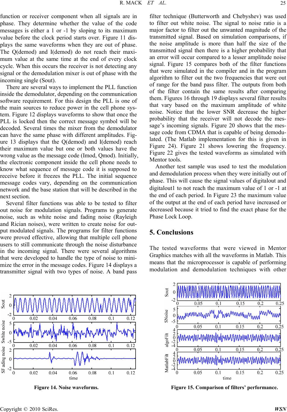 R. MACK ET AL. Copyright © 2010 SciRes. WSN 25 function or receiver component when all signals are in phase. They determine whether the value of the code messages is either a 1 or -1 by sloping to its maximum value before the clock period starts over. Figure 11 dis- plays the same waveforms when they are out of phase. The Q(demod) and I(demod) do not reach their maxi- mum value at the same time at the end of every clock cycle. When this occurs the receiver is not detecting any signal or the demodulation mixer is out of phase with the incoming single (Sout). There are several ways to implement the PLL function inside the demodulato r, depending on the communication software requirement. For this design the PLL is one of the main sources to reduce power in the cell phone sys- tem. Figure 12 displays w aveforms to show that once the PLL is locked then the correct message symbol will be decoded. Several times the mixer from the demodulator can have the same phase with different amplitudes. Fig- ure 13 displays that the Q(demod) and I(demod) reach their maximum value but one or both values have the wrong value as the message code (Imod, Qmod). Initially, the electronic component inside the cell phone needs to know what sequence of message code it is supposed to receive before it freezes the PLL. The initial sequence message codes vary, depending on the communication network and the base station that will be described in the next secti on. Several filter functions was able to be tested to filter out noise for modulation signals. Programs to generate noise, such as white noise and fading noise (Rayleigh and Rician noises), were written to create noise for out- put modulated signals. The programs for filter functions were proved effective, allowing that multiple cell phone users to still communicate through the noise disturbance in the incoming signal. There were several algorithms that were developed to handle the type of noise to mini- mize the error in the message codes. Figure 14 displays a transmitter signal with two types of noise. A band pass filter technique (Butterworth and Chebyshev) was used to filter out white noise. The signal to noise ratio is a major factor to filter out the unwanted magnitude of the transmitted signal. Based on simulation comparisons, if the noise amplitude is more than half the size of the transmitted signal then there is a higher probability that an error will occur compared to a lesser amplitude noise signal. Figure 15 compares both of the filter functions that were simulated in the compiler and in the program algorithm to filter out the two frequencies that were out of range for the band pass filter. The outputs from both of the filter contain the same results after comparing them. Figures 16 through 19 displays several filter results that vary based on the maximum amplitude of white noise. Notice that the lower SNR decrease the higher probability that the receiver will not decode the mes- sage’s incoming signals. Figure 20 shows that the mes- sage code from CDMA that is capable of being demodu- lated. (The Matlab implementation for this is given in Figure 24). Figure 21 shows lowering the frequency. Figure 22 gives the tested waveforms as simulated with Mentor tools. Another test sample was used to test the modulation and demodulation process when they were initially out of phase. This will cause the signal values of digitalout and digitalout1 to not reach the maximum value of 1 or -1 at the end of each period. In Figure 23 the maximum value of the output at the end of each period have increased or decreased because it tried to find the exact phase for the Phase Lock Loop. 5. Conclusions The tested waveforms that were viewed in Mentor Graphics matches with all the waveforms in Matlab. This means that the microprocessor is capable of performing modulation and demodulation techniques with other Figure 14. Noise waveforms. Figure 15. Comparison of filters’ performance.  R. MACK ET AL. 26 Figure 16. White noise 25% of message signal. Figure 17. White noise 100% of message signal. Figure 18. White noise 200% of message signal. Figure 19. White noise 400% of message signal. Copyright © 2010 SciRes. WSN  R. MACK ET AL. 27 Figure 20. CDMA process in Matlab. (a) (b) Figure 21. (a) Lower the frequency; (b) Lower the frequency with noise. C opyright © 2010 SciRes. WSN  R. MACK ET AL. 28 (a) (b) Figure 22. (a) Tested waveforms for the first two periods; (b) Tested waveform while lowering the frequency. Copyright © 2010 SciRes. WSN  R. MACK ET AL. Copyright © 2010 SciRes. WSN 29 Figure 23. Tested waveforms while out of phase. Icdma(samp) = input1a*seqnum(sq); Qcdma(samp) = input1b*seqnum(sq); Icdma2(samp) = input2a*seqnum2(sq); Qcdma2(samp) = input2b*seqnum2(sq); Icdma3(samp) = input3a*seqnum3(sq); Qcdma3(samp) = input3b*seqnum3(sq); Icdma4(samp) = input4a*seqnum4(sq); Qcdma4(samp) = input4b*seqnum4(sq); Icdmat(samp) = Icdma(samp) + Icdma2(samp) + Icdma3(samp) + Icdma4(samp); Qcdmat(samp) = Qcdma(samp) + Qcdma2(samp) + Qcdma3(samp) + Qcdma4(samp); Ss1(samp) = Icdmat(samp)*cos(2*pi*freq*t+ phasein) + Qcdmat(samp)*sin(2*pi*freq*t+ phasein); if(l > longsam) times1(samp1) = t; if(sq ~= 1) IIz(samp1) = II(samp)*seqnum2(sq)+IIz(samp1-1); QQz(samp1) = QQ(samp)*seqnum2(sq)+QQz(samp1-1); else IIz(samp1) = II(samp)*seqnum2(sq); QQz(samp1) = QQ(samp)*seqnum2(sq); end if(sq == 6) IIcdma(samp2)=IIz(samp1); QQcdma(samp2)=QQz(samp1); times2(samp2)=t; samp2=samp2+1; end end Figure 24. Matlab implementation of CDMA. communications systems. Also, since the LEDs outputs from Xilinx matches with the waveforms in Mentor Gra- phics ind icate that the Xilinx can be implemented as cell phone microcontroller or a base station controller. The  R. MACK ET AL. 30 methods were the basic functions that all cellular phones use for communication with the base station. There were ideas that were created to adjust several algorithm func- tions inside the DSP chip to save power. Lowering the frequency is the main method that was developed to save power in DSP chips compared to pipelin ing, parallelism, and reducing several algorithms for several functions such as the cos(x) and sin(x). There are several adjust- ments that might not have been recognized to simulate with the functions inside the main microchip controller. This study proves that these functions work in three dif- ferent real time compilers, which are Matlab, Mentor Graphics, and Xilinx. This proves that these methods can be developed in any type of microchip fabrication fac- tory. The Mach-Pa compiler in Mentor Graphics proves that if the frequency was lowered, it would automatically save power compared to when it is higher. This has been an interesting and challenging project to promote a better understanding of how the communication process work- ed with the base station and cell phones. Other compo- nents to have a better internal knowledge of working with the main microchip are the push buttons, screen display, microphone, speaker, and antenna for every cell phone. 6. References [1] Montanaro, R. T. Witek, K. Anne, A. J. Black, E. M. Cooper, D. W. Dobberpuhl, P. M. Donahue, J. Eno, W. Hoeppner, D. Kruckemyer, T. H. Lee, P. C. M. Lin, L. Madden, D. Murray, M. H. Pearce, S. Santhanam, K. J. Snyder, R. Stehpany, and S. C. Thierauf, “A 160-MHz, 32-b, 0.5-W CMOS RISC microprocessor,” IEEE Journal of Solid-State Circuits, Vol. 31, No. 11, pp. 1703–1714, November 1996. [2] F. M. Gardner, “Phaselock techniques,” 2nd Edition, John Wiley and Sons, New York, NY, 1979. [3] R. Philips, “Low power PLL FM demodulator for sat ellite TV receivers, integrated circuits,” Trenton, NJ, 1996. [4] M. Vesterbacka, “Digit-serial implementation of LDI/ LDD allpass filters,” Scottsdale, AZ, 2001. [5] H. Ming, O. Vainio, and M. Renfors, “Digit-serial design of a wave digital filter,” Proceedings of IEEE Instrumen- tation and Measurement Technology Conference, Vol. 1, pp. 542–545, 1999. [6] A. Fettweis, H. Levin, and A. Sedlmeyer, “Wave digital lattice filters,” International Journal of Circuit Theory and Applications, Vol. 2, pp. 203–211, June 1974. Copyright © 2010 SciRes. WSN |