Materials Sciences and Applications
Vol.06 No.05(2015), Article ID:55848,4 pages
10.4236/msa.2015.65039
Fabrication of Erbium and Ytterbium Co-Doped Tantalum-Oxide Thin Films Using Radio-Frequency Co-Sputtering
Kenta Miura*, Yuki Arai, Kazusa Kano, Osamu Hanaizumi
Graduate School of Science and Technology, Gunma University, Kiryu, Japan
Email: *mkenta@gunma-u.ac.jp
Copyright © 2015 by authors and Scientific Research Publishing Inc.
This work is licensed under the Creative Commons Attribution International License (CC BY).
http://creativecommons.org/licenses/by/4.0/


Received 15 February 2015; accepted 20 April 2015; published 21 April 2015
ABSTRACT
An erbium and ytterbium co-doped tantalum-oxide (Ta2O5:Er, Yb) thin film was fabricated using a simple co-sputtering method for the first time, and its photoluminescence (PL) spectrum was evaluated. Energy transfers between Er3+ and Yb3+ in the Ta2O5:Er, Yb co-sputtered thin film were discussed by comparing between PL spectra of the Ta2O5:Er, Yb film and Ta2O5:Er or Ta2O5:Yb films reported in our previous works. Such a Ta2O5:Er, Yb co-sputtered film can be used as a high-refrac- tive-index and light-emitting material of a multilayered photonic crystal that can be applied to a novel light-emitting device, and it will also be used as a multi-functional coating film having both anti-reflection and down-conversion effects for realizing a high-efficiency silicon solar cell.
Keywords:
Tantalum Oxide, Erbium, Ytterbium, Co-Sputtering, Photoluminescence

1. Introduction
Many studies on rare-earth-doped tantalum (V) oxide (Ta2O5) have been conducted because Ta2O5 is a potential host material for new phosphors due to its low phonon energy (100 - 450 cm−1) compared with other oxide materials such as SiO2 [1] . Visible photoluminescence (PL) from erbium-doped Ta2O5 (Ta2O5:Er) produced by the sol-gel method [2] [3] and ion implantation [4] has been reported. Their PL spectra have main peaks at a wavelength of 550 nm due to the 4S3/2→4I15/2 transition of Er3+, and at a wavelength of 670 nm due to the 4F9/2→4I15/2 transition of Er3+. We previously demonstrated that Ta2O5:Er thin films deposited using a simple co-sputtering method exhibited such PL peaks at wavelengths of 550 and 670 nm after annealing at 600˚C to 1100˚C [5] [6] . Recently, we also fabricated ytterbium-doped Ta2O5 (Ta2O5:Yb) thin films using the same co-sputtering method in order to expand the useful wavelength range of our rare-earth-doped and light-emitting Ta2O5 co-sputtered films [7] . We observed PL spectra having sharp peaks at a wavelength of 980 nm from the Ta2O5:Yb thin films after annealing at 700˚C to 1000˚C [7] . The 980-nm peaks seemed to be the result of the 2F5/2→2F7/2 transition of Yb3+ [7] .
Furthermore, in our recent works, we demonstrated Tm and Ce co-doped Ta2O5 (Ta2O5:Tm, Ce) [8] , Er and Ce co-doped Ta2O5 (Ta2O5:Er, Ce) [9] , and Er, Eu, and Ce co-doped Ta2O5 (Ta2O5:Er, Eu, Ce) [10] thin films prepared using the co-sputtering method. In this work, we fabricated an Er and Yb co-doped Ta2O5 (Ta2O5:Er, Yb) thin film using radio-frequency (RF) magnetron co-sputtering of Ta2O5, Er2O3, and Yb2O3 for the first time, and evaluated its PL property.
2. Experimental
A Ta2O5:Er, Yb thin film was prepared using our co-sputtering method reported in [5] -[13] . A Ta2O5 disc (99.99% purity, diameter 100 mm), two Er2O3 pellets (99.9% purity, diameter 21 mm), and two Yb2O3 pellets (99.9% purity, diameter 21 mm) were used as co-sputtering targets. The Er2O3 and Yb2O3 pellets were placed on the Ta2O5 disc as shown in Figure 1. The film was deposited using a RF magnetron sputtering system (ULVAC, SH-350-SE). The flow rate of Ar gas introduced into the vacuum chamber was 10 sccm, and the RF power supplied to the targets was 200 W. A fused-silica plate (1 mm thick) was used as a substrate, and it was not heated during co-sputtering. We subsequently annealed the film in ambient air at 900˚C for 20 min using an electric furnace (Denken, KDF S-70). The PL spectrum of the Ta2O5:Er, Yb film was measured using a dual-grating monochromator (Roper Scientific, SpectraPro 2150i) and a CCD detector (Roper Scientific, Pixis:100B, electrically cooled to −80˚C) under excitation with a He-Cd laser (Kimmon, IK3251R-F, wavelength λ = 325 nm).
3. Results and Discussion
Figure 2 presents PL spectra of Ta2O5:Er, Yb (red line) and Ta2O5:Er (without Yb, black line) [5] [6] co-sput- tered thin films. We observed typical PL peaks around wavelengths of 550, 670, 850, and 980 nm from both the films. The 550-, 670-, and 850-nm peaks seem to be the results of the 4S3/2→4I15/2, 4F9/2→4I15/2, and 4I9/2→4I15/2 transitions of Er3+, respectively [5] [14] [15] . The 980-nm peaks seem to be the results of the 4I11/2→4I15/2 transition of Er3+ or the 2F5/2→2F7/2 transition of Yb3+ [7] [14] -[16] . From Figure 2, we can find that the 550-, 670-, and 850-nm peaks from the Ta2O5:Er film decreased by Yb doping. In contrast, the intensity of the 980-nm peak from the Ta2O5:Er, Yb film was stronger than that from the Ta2O5:Er film. This seems to be because of overlapping between the above-mentioned 4I11/2→4I15/2 transition of Er3+ and the 2F5/2→2F7/2 transition of Yb3+, and energy transfers from Er3+ to Yb3+ reported in [14] . Figure 3 illustrates energy level diagrams of Er3+ and Yb3+ [14] [15] . The energies of 4S3/2 (the origin of the 550-nm peak), 4F9/2 (the origin of the 670-nm peak), and 4I9/2 (the origin of the 850-nm peak) states of Er3+ seem to transfer through the 4I11/2 state of Er3+ to the 2F5/2 state of Yb3+ as presented in Figure 3.

Figure 1. Schematic diagram of the sputtering target for co- sputtering of Er2O3, Yb2O3, and Ta2O5 used in this work.
Figure 4 presents PL spectra of the same Ta2O5:Er, Yb film (red line) and a Ta2O5:Yb film (without Er, green line) reported in [7] . The 980-nm peak from the Ta2O5:Yb film is much stronger than that from the Ta2O5:Er, Yb film. This seems to be because the opposite energy transfer from Yb3+ to Er3+ occurred in the Ta2O5:Er, Yb film. The energy of the 2F5/2 state of Yb3+ partially transfer to the 4I11/2 state of Er3+ at first, and subsequently relax to the 4I13/2 state as presented in Figure 3. Finally light emission around a wavelength of 1550 nm due to the 4I13/2→4I15/2 transition of Er3+ seems to occur [14] . The 1550-nm emission may cause the decrease of the 980- nm-peak intensity. Unfortunately, our detector did not detect the light emission in the wavelength range. We will try to evaluate the light-emission properties of our Ta2O5:Er, Yb films in the near-infrared range in order to make the mechanism of the energy transfer between Er3+ and Yb3+ clearer.
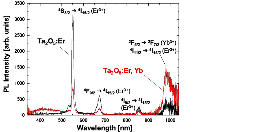
Figure 2. PL spectra of Ta2O5:Er, Yb and Ta2O5:Er [5] [6] co-sputtered thin films.

Figure 3. Energy level diagrams of Er3+ and Yb3+ [14] [15] .

Figure 4. PL spectra of Ta2O5:Er, Yb and Ta2O5:Yb [7] co-sputtered thin films.
Such a Ta2O5:Er, Yb co-sputtered thin film can be used as a high-refractive-index and light-emitting material of a multilayered photonic crystal that can be applied to a novel light-emitting device [17] , and it will also be used as a multi-functional coating film having both anti-reflection [18] and down-conversion [14] -[16] effects for realizing a high-efficiency silicon solar cell.
4. Summary
A Ta2O5:Er, Yb thin film was fabricated using our simple co-sputtering method for the first time, and its PL spectrum was evaluated. Energy transfers between Er3+ and Yb3+ in our Ta2O5:Er, Yb co-sputtered film were discussed by comparing between PL spectra of the film and our Ta2O5:Er or Ta2O5:Yb films. Such a Ta2O5:Er, Yb co-sputtered thin film can be used as a high-refractive-index and light-emitting material of a multilayered photonic crystal that can be applied to a novel light-emitting device, and it will also be used as a multi-func- tional coating film having both anti-reflection and down-conversion effects for realizing a high-efficiency silicon solar cell.
Acknowledgements
Part of this work was supported by the “Element Innovation” Project by Ministry of Education, Culture, Sports, Science and Technology in Japan; and JSPS KAKENHI Grant Number 26390073. Part of this work was conducted at the Human Resources Cultivation Center (HRCC), Gunma University, Japan.
References
- Sanada, T., Wakai, Y., Nakashita, H., Matsumoto, T., Yogi, C., Ikeda, S., Wada, N. and Kojima, K. (2010) Preparation of Eu3+-Doped Ta2O5 Phosphor Particles by Sol-Gel Method. Optical Materials, 33, 164-169. http://dx.doi.org/10.1016/j.optmat.2010.08.018
- Kojima, K., Yoshida, S., Shiraishi, H. and Maegawa, A. (1995) Green Upconversion Fluorescence in Er3+-Doped Ta2O5 Heated Gel. Applied Physics Letters, 67, 3423-3425. http://dx.doi.org/10.1063/1.115267
- Wada, N., Kubo, M., Maeda, N., Akira, M. and Kojima, K. (2004) Fluorescence Property and Dissolution Site of Er3+ in Ta2O5 Film Prepared by Sol-Gel Method and Dip-Coating Technique. Journal of Materials Research, 19, 667-675. http://dx.doi.org/10.1557/jmr.2004.19.2.667
- Rigneault, H., Flory, F., Monneret, S., Robert, S. and Roux, L. (1996) Fluorescence of Ta2O5 Thin Films Doped by Kilo-Electron-Volt Er Implantation: Application to Microcavities. Applied Optics, 35, 5005-5012. http://dx.doi.org/10.1364/AO.35.005005
- Singh, M.K., Fusegi, G., Kano, K., Bange, J.P., Miura, K. and Hanaizumi, O. (2009) Intense Photoluminescence from Erbium-Doped Tantalum Oxide Thin Films Deposited by Sputtering. IEICE Electronics Express, 6, 1676-1682. http://dx.doi.org/10.1587/elex.6.1676
- Singh, M.K., Miura, K., Fusegi, G., Kano, K. and Hanaizumi, O. (2013) Visible-Light Emission Properties of Erbium- Doped Tantalum-Oxide Films Produced by Co-Sputtering. Key Engineering Materials, 534, 154-157. http://dx.doi.org/10.4028/www.scientific.net/KEM.534.154
- Miura, K., Kano, K., Arai, Y. and Hanaizumi, O. (2015) Preparation of Light-Emitting Ytterbium-Doped Tantalum- Oxide Thin Films Using a Simple Co-Sputtering Method. Materials Sciences and Applications, 6, 209-213. http://dx.doi.org/10.4236/msa.2015.62024
- Miura, K., Osawa, T., Yokota, Y., Suzuki, T. and Hanaizumi, O. (2015) Photoluminescence Properties of Thulium and Cerium Co-Doped Tantalum-Oxide Films Prepared by Radio-Frequency Co-Sputtering. Materials Sciences and Applications, 6, 263-268. http://dx.doi.org/10.4236/msa.2015.64031
- Miura, K., Osawa, T., Suzuki, T., Yokota, Y. and Hanaizumi, O. (2015) Fabrication and Evaluation of Green-Light Emitting Ta2O5:Er, Ce Co-Sputtered Thin Films. Results in Physics, 5, 78-79. http://dx.doi.org/10.1016/j.rinp.2015.02.002
- Miura, K., Osawa, T., Suzuki, T., Yokota, Y. and Hanaizumi, O. (2015) Yellow Light Emission from Ta2O5:Er, Eu, Ce Thin Films Deposited Using a Simple Co-Sputtering Method. Results in Physics, 5, 26-27. http://dx.doi.org/10.1016/j.rinp.2014.11.003
- Miura, K., Arai, Y., Osawa, T. and Hanaizumi, O. (2012) Light-Emission Properties of Europium-Doped Tantalum- Oxide Thin Films Deposited by Radio-Frequency Magnetron Sputtering. Journal of Light and Visual Environment, 36, 64-67. http://dx.doi.org/10.2150/jlve.36.64
- Miura, K., Osawa, T., Yokota, Y., Suzuki, T. and Hanaizumi, O. (2014) Fabrication of Tm-Doped Ta2O5 Thin Films Using a Co-Sputtering Method. Results in Physics, 4, 148-149. http://dx.doi.org/10.1016/j.rinp.2014.08.011
- Miura, K., Osawa, T., Yokota, Y. and Hanaizumi, O. (2014) Fabrication and Evaluation of Ta2O5:Y2O3 Co-Sputtered Thin Films. Results in Physics, 4, 185-186. http://dx.doi.org/10.1016/j.rinp.2014.09.004
- Rodriguez, V.D., Tikhomirov, V.K., Mendez-Ramos, J., Yanes, A.C. and Moshchalkov, V.V. (2010) Towards Broad Range and Highly Efficient Down-Conversion of Solar Spectrum by Er3+-Yb3+ Co-Doped Nano-Structured Glass- Ceramics. Solar Energy Materials and Solar Cells, 94, 1612-1617. http://dx.doi.org/10.1016/j.solmat.2010.04.081
- Aarts, L., van der Ende, B.M. and Meijerink, A. (2009) Downconversion for Solar Cells in NaYF4:Er, Yb. Journal of Applied Physics, 106, Article ID: 023522. http://dx.doi.org/10.1063/1.3177257
- Ueda, J. and Tanabe, S. (2011) Broadband near Ultra Violet Sensitization of 1 μm Luminescence in Yb3+-Doped CeO2 Crystal. Journal of Applied Physics, 110, Article ID: 073104. http://dx.doi.org/10.1063/1.3642984
- Hanaizumi, O., Miura, K., Saito, M., Sato, T., Kawakami, S., Kuramochi, E. and Oku, S. (2000) Frontiers Related with Automatic Shaping of Photonic Crystals. IEICE Transactions on Electronics, E83-C, 912-919.
- Cid, M., Stem, N., Brunetti, C., Beloto, A.F. and Ramos, C.A.S. (1998) Improvements in Anti-Reflection Coatings for High-Efficiency Silicon Solar Cells. Surface and Coatings Technology, 106, 117-120. http://dx.doi.org/10.1016/S0257-8972(98)00499-X
NOTES

*Corresponding author.