Journal of Modern Physics
Vol.06 No.02(2015), Article ID:53884,5 pages
10.4236/jmp.2015.62012
Electronic Transport through a Graphene Nanoribbon Composed of Nanoribbons of Different Widths
Wen Liu1, Jie Cheng1, Jianhua Zhao1, Desheng Liu1,2
1Physics and Information Engineering Department, Jining University, Qufu, China
2School of Physics, Shandong University, Jinan, China
Email: liuwenjnxy@163.com
Copyright © 2015 by authors and Scientific Research Publishing Inc.
This work is licensed under the Creative Commons Attribution International License (CC BY).
http://creativecommons.org/licenses/by/4.0/


Received 21 January 2015; accepted 6 February 2015; published 10 February 2015
ABSTRACT
Based on non-equilibrium Green’s function method combined with the density functional theory, we have studied the electronic properties of a graphene nanoribbon (GNR) which is composed of two GNRs with different widths. The results show that the electron transmission is greatly modulated by the applied bias. The current of the system displays negative differential resistance effect, which is attributed to the broadening of the transmission gap with the increase of the bias around the Fermi level.
Keywords:
Graphene Nanoribbon, Electronic Transport, Negative Differential Resistance

1. Introduction
In recent years, considerable efforts have been devoted to mesoscopic devices [1] [2] . With the great advancement in preparation and synthesis techniques, carbon-based nanostructures have emerged as one of the most promising candidates for nanoelectronics. Much attention has been paid to developing graphene electronics. Narrow graphene nanoribbons (GNRs) have been realized in recent experiments [3] . Their interesting electronic properties, such as the giant carrier mobility at room temperature [4] , the anomalous quantum hall effect [5] , and quantum blockade [6] , indicate remarkable application in graphene-based devices. A large amount of works have been devoted to theoretical studies on the electronic transport properties of GNRs [7] - [9] .
It has been known that the electronic properties of a GNR are sensitive to its width, edges and defects. By fusing an armchair GNR (AGNR) and a zigzag GNR (ZGNR) side by side, Li et al. have constructed a GNR heterojunction, the electronic transport properties which have been investigated with the first principles method. Intrinsic rectification behaviors have been observed, which depend on the width of the nanoribbon and are largely sensitive to the connection length between ZGNR and AGNR [10] . A hybrid graphane/grephene nanori- bbon is built by substituting zigzag graphane nanoribbon into ZGNR. It is found that the transport properties of the pristine ZGNRs can be effectively modulated by the substitution, and this modulation is sensitive to the concentration of the substituted graphane region [11] . Due to the metallic or semiconductor nature of GNRs with different widths, Naumis et al. proposed an idea of joining different sections of AGNRs in order to construct a field effect transistor of a resistance [12] . Motivated by that, we aim to build nanoribbons by joining ZGNRs of different widths and investigate their electronic transport properties with the first principles method. As it turns out, we find negative differential resistance (NDR) behaviors in such a system.
2. Ease of Use
In Figure 1 we present the structure of our proposed nanoribbon, which is made from two sections of ZGNRs with different widths. Following previous convention, GNR with zigzag edges can be labeled as N-ZGNR with N the number of zigzag lines across the ribbon width. We denote the narrower part as 4-ZGNR and the wider one as 6-ZGNR. The connected nanoribbon is denoted as 4-ZGNR/6-ZGNR. Hydrogen is used to saturate the dangling bonds at the edges and to make the system more stable. In our calculation, the geometry of 4-ZGNR/ 6-ZGNR is first optimized with a residual force of 0.05 eV/Å. It can be seen that a section of the left electrode and a section of the right electrode have been included in the central scattering region to avoid direct coupling between these two electrodes. After the structure relaxation, we calculate the electronic transport properties of the system by the well test ATK package, which adopts a non-equilibrium Green function (NEGF) method combined with density functional theory (DFT). The double-zeta polarization (DZP) basis set for valence electrons is adapted. The Perdew-Burke-Ernzerhof (PBE) formulation of the generalized gradient approximation (GGA) exchange correlation function is used. The electronic Brillouin zone integration is sampled with a 1 × 1 × 100 uniform k-point mesh. The current is calculated using the Landauer-Büttiker formula (1):
 (1)
(1)
where  is the transmission coefficient for electrons with energy E at bias voltage
 ,
,  the Fermi function, and
  the electrochemical potential of the left/right electrode.
3. Results and Discussion
In Figure 2 we illustrate the calculated energy dependence of the zero-bias transmission spectrum  of 4-ZGNR/6-ZGNR. The transmission spectrum is almost symmetry about the Fermi level. There is a dip at the Fermi level. Large transmission platforms continue until the energy reach ±1.9 eV, and then the transmission coefficient undergoes drastic increase. For the pristine 4-ZGNR and 6-ZGNR counterparts of 4-ZGNR/6-ZGNR, the transmission spectra of which are illustrated in Figure 3. One can find that neither of them has a dip around the Fermi level and we attribute the dip that appear in 4-ZGNR/6-ZGNR to the resonant scattering induced by the 4-ZGNR and 6-ZGNR interface.

Figure 1. The schematic device model of 4-ZGNR/6-ZGNR and the shadow parts are used as left and right surface layers.

Figure 2. The energy dependence of the zero-bias transmission spectrum T(E) of 4-ZGNR/6-ZGNR.

Figure 3. The energy dependence of the zero-bias transmission spectra T(E) of 4-ZGNR (a) and 6-ZGNR (b). The insets are the schematics of 4-ZGNR and 6-ZGNR.
The electronic properties can be examined by calculating the I-V characteristic curve of the system, as shown in Figure 4. It can be seen that from the negative bias 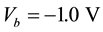 to positive bias
 , which is reasonable in practical experimental measurements, the I-V curve is asymmetrical. This is physically due to the inherent asymmetrical structure of the system. It is known that GNRs with hydrogen passivated edges have nonzero and direct band gaps, and the ribbon widths and energy band gaps are related to each other in inverse proportion. For the nanoribbon 4-ZGNR/6-ZGNR, the calculated energy gap is small of 0.2 eV. Therefore, once the bias is applied the current begins to increase. As the bias increases from
  to
to , the current enhancement is nearly linear. Then a current platform continues until the bias is increased up to
 . An interesting point one can find is the negative differential resistance (NDR) phenomenon. The current decreases when the bias increases from
  to
to , both in the negative and positive directions.
As the current is obtained from the Landauer-Büttiker formula mentioned above, the magnitude of current in fact depends on the transmission coefficient in the integral regions, namely, the size of the integral area in the bias window. Therefore, to further understand the change of the current, we can turn to the bias dependence of  which is plotted in Figure 5. The dashed lines denote the corresponding bias windows at different biases. It can be found that the transport properties of 4-ZGNR/6-ZGNR are remarkably modulated by the bias. Without the bias applied, there is a dip around the Fermi level. As the bias increases, the dip involves into a transmission gap, which becomes wider with the enhancement of the bias. The zero value of transmission coefficients correspond to the resonant backscattering states. The effect of resonant backscattering results in a full suppression

Figure 4. The I-V curve of 4-ZGNR/6-ZGNR in the bias range (−1.0 V, 1.0 V).

Figure 5. The bias evolution of the transmission spectrum T(E). The dashed lines denote the bias windows under corresponding biases.
of the single available conduction channel at a certain resonance energy. An obvious difference in  at
at , 1.0 V is that small and broad conductance peaks are observed in the energy range (−0.1 eV, 0.3 eV) and (−0.3 eV, 0.0 eV), respectively, which will induce the enhancement of the transmission conductance around the Fermi level. Local density of states (LODS) analysis can provide us with the information of the distribution of electron channels at certain energy level of the system in real space. To clarify the origin of the transmission peaks in the transmission gaps mentioned above as shown in Figure 5(d) and Figure 5(e), we analyze the LDOS of the system within the energy window (−0.3 eV, 0.0 eV) at
 . Figure 6 shows the LDOS at two energy levels
 , −0.30 eV within the energy window. For comparison, we also illustrate the LDOS at the same energy levels under
  in Figure 6. It can be seen from Figure 6(a) that the LDOS at
 , −0.30 eV mainly concentrate on the middle part of the system and the carbon atoms in the left

 (a) (b)
Figure 6. (Color online) LDOS for 4-ZGNR/6-ZGNR under Vb = 1.0 V (a) and Vb = 0.4 V (b) at E = −0.23, 0.30 eV from top to bottom.
side of the 4-ZGNR part, respectively. Although the LDOS is not well delocalized, it is much larger than that under  at the same energy levels as shown in Figure 6(b), from which we find that the LDOS distribution on every atom is nearly zero. That is why a small but broad transmission peak appear around the Fermi level at
 . For the peak appearing in the energy range (−0.1 eV, 0.3 eV), we can do the same analysis.
In the bias range from  to
to , although the transmission gap inside the bias window becomes larger as the bias increases, the total integral area of transmission coefficients enlarges, and so the current goes up. The situation is the same for the negative bias from
  to
to . However, when the bias is further increased from 0.8 V to 1.0 V and from −0.8 V to −1.0 V, despite that the bias window enlarges and a broad transmission peak appears in (−0.3 eV, 0.0 eV), it can not compensate the influence induced by the increase of the transmission gap, which leads to the result that the integral area of the transmission coefficients decrease, i.e., the current is reduced and NDR phenomenon appears.
4. Summary
In summary, we have built a GNR by combining two GNRs with different widths and the electronic transport properties which are investigated by the first principles method. The numerical calculation indicates that the electron transmission shows a great dependence on the applied bias. With the increase of the bias, the transmission gap around the Fermi level broadens, which reduces the transmission conductance around the Fermi level. NDR is observed in such a system, the origin for which we attribute to the broadening of the transmission gap with the increase of the bias around the Fermi level.
Acknowledgements
Liu Wen thanks the support from the National Natural Science Foundation of China (Grant No. 11074146), Shandong Province Higher Educational Science and Technology Program (Grant No. J13LJ53) and the Natural Science Foundation of Shandong Province (No. ZR2014AL013).
References
- Liu, Y.L., Deng, X.Q. and Duan, X.C. (2013) Physica E, 52, 21-26. http://dx.doi.org/10.1016/j.physe.2013.03.016
- Li, P.W., Yang, Z., Zhang, W.D. and Xiong, S.J. (2013) Journal of Molecular Structure, 1038, 1-7. http://dx.doi.org/10.1016/j.molstruc.2013.01.022
- Han, M.Y., Özyilmaz, B., Zhang, Y.B. and Kim, P. (2007) Physical Review Letters, 98, Article ID: 206805 http://dx.doi.org/10.1103/PhysRevLett.98.206805
- Morozov, S.V., Novoselov, K.S. and Katsnelson, M.I. (2008) Physical Review Letters, 100, 016602-016604. http://dx.doi.org/10.1103/PhysRevLett.100.016602
- Geim, A.K. and Novoselov, K.S. (2007) Nature Materials, 6, 183-191. http://dx.doi.org/10.1038/nmat1849
- Zhang, Y.Y., Hu, J.P., Bernevig, B.A. and Wang, X.R. (2008) Physical Review B, 78, 155413-155418. http://dx.doi.org/10.1103/PhysRevB.78.155413
- Min, Y., Fang, H.J. and Dong, Z.C. (2013) Physica B, 430, 40-44. http://dx.doi.org/10.1016/j.physb.2013.08.027
- Min, Y., Fang, H.J. and Zhong, C.G. (2013) International Journal of Modern Physics B, 27, 1350081-1350086. http://dx.doi.org/10.1142/S0217979213500811
- Tang, G.P., Zhou, J.C., Zhang, Z.H., Deng, X.Q. and Fan, Z.Q. (2013) Carbon, 60, 94-101. http://dx.doi.org/10.1016/j.carbon.2013.04.002
- Li, X.F., Wang, L.L., Chen, K.Q. and Luo, Y. (2012) Journal of Physics: Condensed Matter, 24, 095801-095805. http://dx.doi.org/10.1088/0953-8984/24/9/095801
- Zou, W., Yu, Z.Z., Zhang, C.X., Zhong, J.X. and Sun, L.Z. (2012) Applied Physics Letters, 100, 103109-103111. http://dx.doi.org/10.1063/1.3692725
- Naumis, G.G., Terrones, M., Terrones, H. and Gaggero-Sager, L.M. (2009) Applied Physics Letters, 95, 182104- 182106. http://dx.doi.org/10.1063/1.3257731