Double-Sided Microstrip Circular Antenna Array for WLAN/WiMAX Applications ()
1. Introduction
Ultra-wideband (UWB: 3.1 to 10.6 GHz) frequency spectrum has been approved by the US Federal Communications Commission (FCC) for unlicensed short range wireless communications since 2002. In this frequency range, wireless local-area network (WLAN) IEEE802.11a and HIPERLAN/2 WLAN operates in 5.0 - 6.0 GHz band. In some European and Asian countries, world interoperability for microwave access (WiMAX) service is provided in the frequency range of 3.3 - 3.6 GHz [1-4]. To support the WLAN/WiMAX application, antenna arrays that provide omnidirectional radiation pattern are required. To respond to this need, recent antenna design efforts were focused on omnidirectional antennas with high gain and no sidelobes [5-8]. Rectangular arrays are common type used for antenna arrays. Studies on dual band antennas employing rectangular arrays were reported [9-12]. Compared to rectangular patch antenna arrays, there are limited numbers of studies performed on circular patch antenna arrays due to difficulties in fabrication [13]. Advantages of circular antenna array include high gain and narrow beam width [13].
In this paper, a new microstrip circular antenna arrays were designed, fabricated, and characterized to provide omnidirectional radiation pattern for WLAN/WiMAX applications. Two antenna arrays were designed—one for single band at 2.45 GHz and the other for dual bands at 3.3 - 3.6 GHz and 5.0 - 6.0 GHz. For single band operation, circular patch array was placed on the top layer of the microtrip and a small rectangular patch was placed on the bottom layer for ground connection. For dual band operation, similar circular patch array was placed on both top and bottom layers of the microstrip with larger rectangular patch placed on the bottom layer. Both single band (single sided) and dual band (double-sided) microstrip antenna arrays provided desirable antenna characteristics for the intended application.
2. Design and Simulation
2.1. Single-Band Antenna at 2.45 GHz
The configuration of the proposed single band antenna at 2.45 GHz is shown in Figure 1. It consists of six circular patches which are placed only on the top layer. The small rectangular patch is placed on the bottom layer for ground connection.
The directivity for the circular patch antenna is
 (1)
(1)
 (a) (b) (c)
Figure 1. Configuration of the proposed antenna for single band at 2.45 GHz: (a) Top layer; (b) Bottom layer; (c) Top and bottom layers overlaid.
 (2)
(2)
 (3)
(3)
 (4)
(4)
 (5)
(5)
 (6)
(6)
where  is the effective radius,
  is the actual radius,
  is the relative permittivity of the microstrip dielectric substrate,
  is the height of the microstrip substrate, and
  and
and  are Bessel functions.
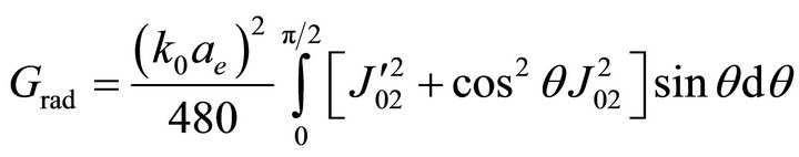
The gain of the antenna was calculated using
 (7)
(7)
 (8)
(8)
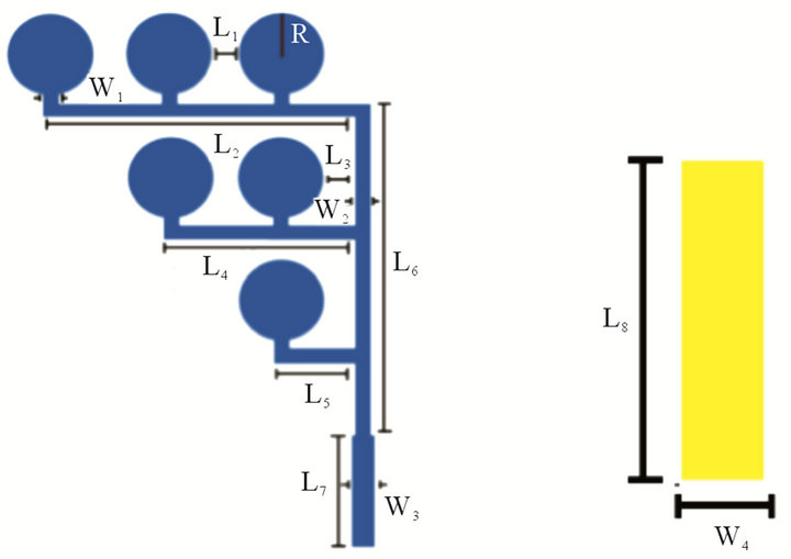
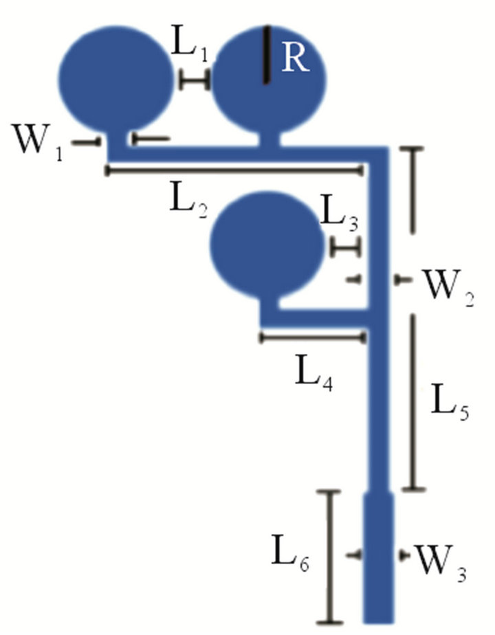
The variable corresponding to each dimensions and values for the dimensions of the proposed antenna are shown in Figure 2 and Table 1, respectively. Here, L, W, and R represent the length, the width, and the radius of the circular patch, respectively.
The gain of the proposed antenna shown in Figure 1 was calculated using (1) - (8) and the dimensions were optimized using ADS [14] which resulted in gain of 3.5 dBi at 2.45 GHz.
2.2. Dual-Band Antenna at 3.3 - 3.6 and 5.0 - 6.0 GHz
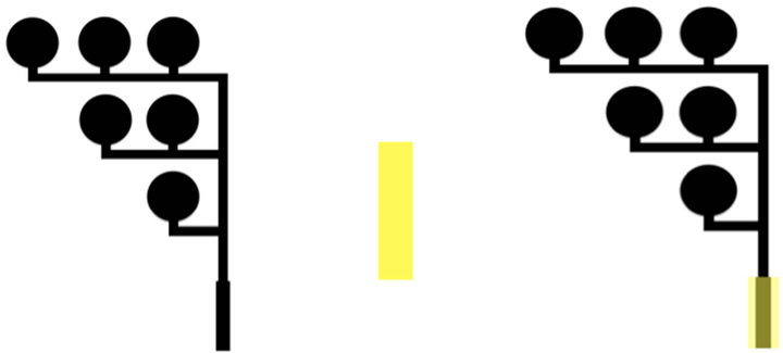
The configuration for the doubled-sided microstrip dual band antenna is shown in Figure 3. The proposed microstrip antenna has circular arrays both on the top and bottom layers. It consists of three circular patched on each layer.
 (a) (b)
Figure 2. Variables corresponding to each dimension of the proposed single band antenna: (a) Top layer; (b) Bottom layer.

Table 1. Dimensions for the proposed single band antenna at 2.4 GHz.
 (a) (b) (c)
Figure 3. Configuration of the proposed antenna for dual band at 3.3 - 3.6 and 5.0 - 6.0 GHz: (a) Top layer; (b) Bottom layer; (c) Top and bottom layers overlaid.
The configuration in Figure 3(a) is similar to the top layer of the single band antenna as shown in Figure 1(a) but with less circular patches. However, the bottom layer in Figure 3(b) is different compared to the bottom layer of the single band antenna shown in Figure 1(b). The double-side nature of the antenna provides dual band characteristics. Identical equations were used for the single band antenna were employed in the design process. The variable corresponding to each dimensions and the dimensions for the proposed dual band antenna are shown in Figure 4 and Table 2, respectively.
Simulation was performed using ADS for the configuration shown in Figure 3(c). The simulated gains of the proposed dual band antenna were 4.0 dBi at 3.45 GHz and 3.3 dBi at 5.5 GHz. The double-sided configuration of the antenna provided higher gain compared to the singled-sided antenna.
3. Measurement Results and Discussions
3.1. Single-Band Atnenna at 2.45 GHz
The antennas were fabricated using LPKF Protomat [15] on FR-4 material with height of 1.524 mm. The photos of the fabricated single band antenna are shown in Figure 5 which has a size of 6.7 × 4.4 (in cm).
Figure 6 shows the comparison between the simulated and the measured S11 results.
The measured operating frequency is close to 2.45 GHz with S11 value below −15 dB. The 3 dB bandwidth at 2.45 GHz was approximately 18%. The measurement and simulation are in fairly good agreement, and the differences are due to microstrip loss and fabrication errors.
Figure 7 shows the comparison between the simulated and measured radiation pattern in xy-plane at 2.45 GHz which is close to omnidirectional pattern.
 (a)
(a)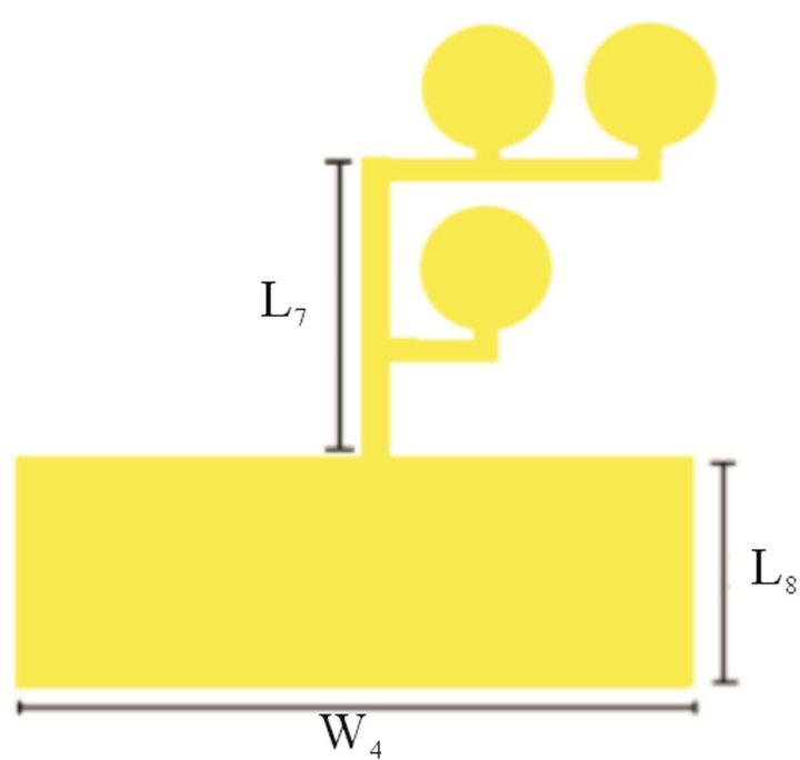 (b)
(b)
Figure 4. Variables corresponding to each dimension of the proposed dual-band antenna: (a) Top layer; (b) Bottom layer.

Table 2. Dimensions for the proposed dual band antenna at 3.3 - 3.6 and 5.0 - 6.0 GHz.
 (a) (b)
Figure 5. Photo of the fabricated single-band antenna: (a) Top layer; (b) Bottom layer.

Figure 6. Simulated and measured return loss for the proposed single-band antenna.
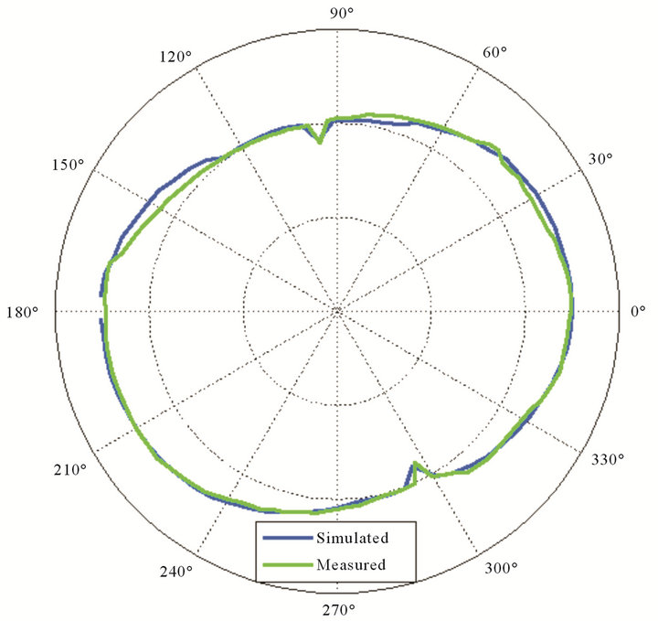
Figure 7. Simulated and measured radiation pattern in xy-plane (coordinate system shown in Figure 5) at 2.45 GHz.
3.2. Dual-Band Antenna at 3.3 - 3.6 and 5.0 - 6.0 GHz
The antennas were fabricated using LPKF Protomat [15]
on double-sided FR-4 materials. The photos of the fabricated dual band antenna are shown in Figure 8 which has a size of 6.6 × 5.2 (in cm).
Figure 9 shows the comparison between the simulated
 (a) (b)
Figure 8. Photo of the fabricated dual-band antenna: (a) Top layer; (b) Bottom layer.
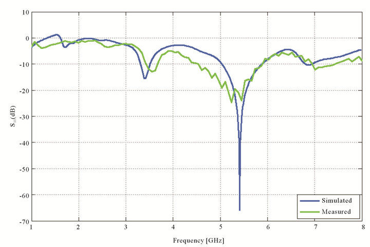
Figure 9. Simulated and measured return loss for the dual band antenna.
and the measured S11 results.
The measured S11 shows dual band near the designed bands with S11 values below −10 dB for both bands. The simulated and measured results give fairly good agreement, and the differences are due to board loss and fabrication errors.
Figure 10 shows the comparison between the simulated and measured radiation pattern in xy-plane at 3.45 and 5.5 GHz which is close to omnidirectional pattern.