Circuits and Systems
Vol.07 No.09(2016), Article ID:68710,6 pages
10.4236/cs.2016.79210
Error Correction Circuit for Single-Event Hardening of Delay Locked Loops
S. Balaji1, S. Ramasamy2
1Department of ECE, Loyola-ICAM College of Engineering and Technology, Tamilnadu, India
2Department of ECE, RMK Engineering College, Tamilnadu, India

Copyright © 2016 by authors and Scientific Research Publishing Inc.
This work is licensed under the Creative Commons Attribution International License (CC BY).
http://creativecommons.org/licenses/by/4.0/


Received 3 May 2016; accepted 20 May 2016; published 20 July 2016
ABSTRACT
In scaled CMOS processes, the single-event effects generate missing output pulses in Delay-Locked Loop (DLL). Due to its effective sequence detection of the missing pulses in the proposed Error Correction Circuit (ECC) and its portability to be applied to any DLL type, the ECC mitigates the impact of single-event effects and completes its operation with less design complexity without any concern about losing the information. The ECC has been implemented in 180 nm CMOS process and measured the accuracy of mitigation on simulations at LETs up to 100 MeV-cm2/mg. The robustness and portability of the mitigation technique are validated through the results obtained by implementing proposed ECC in XilinxArtix 7 FPGA.
Keywords:
Delay-Locked Loop, Single Event Transients, Error Correction Circuit

1. Introduction
Advanced clock networks are required in space application for implementation of data handling, communications and attitude orbit control subsystems. With the limited availability of space-qualified clock networking and frequency control, a fully integrated radiation-hardened clock generator solution is needed. Mostly clock generator employs a Phase-Locked loop (PLL), with stability issues much thwarting in harsh environment and design complexity has made Delay-Locked Loop (DLL) as a viable alternate for clock generator in stern space environment.
The Single-Event Transients (SETs) caused by energetic particle strikes are of increasing concern for the circuits working in radiation environments. The SETs taking place within a DLL are of particular concern as it could corrupt the clock or data-transfer across entire distribution networks, possibly leading to spacecraft failure [1] . In SET characterization of DLL found the Voltage Controlled Delay Line (VCDL) as most sensitive sub- circuit followed by Charge Pump (CP). The VCDL of the DLL generates missing pulses [1] at the output of the DLL. The standard Radiation Hardening By Design (RHBD) techniques like Dual-Modular Redundancy (DMR) and Triple-Modular Redundancy (TMR) [2] have area penalties. In the literature, hardening of VCDLs has been explored to mitigate the missing pulse errors. The VCDL utilizing complementary differential pair delay cells was proposed in [1] was observed to have missing pulses at frequencies above 1 GHz, due to lower critical charge as a result of technology scaling. A peeled VCDL design with a missing-pulse detection and correction block was proposed in [3] mitigated the missing pulses with high design complexity and can be only applied to DLL with two complementary VCDL outputs.
The method proposed in this paper simplifies the Single Event Hardened (SEH)technique from [3] while maintaining performance, and generalises the technique from [3] to be able to applied DLL with both single and differential ended VCDL.
2. Single-Event Error Correction Circuit
Figure 1 introduces a proposed SEH-DLL which can simultaneously detect and mitigate the missing pulses with the proposed Single-Event Error Correction Circuit (SE-ECC) shown in Figure 2. The SE-ECC can be used in DLL with any VCDL topology. In this work the ECC is applied on the VCDL topology used in [4] . The SE-ECC is implemented using an Overlapping Sequence Detector(OSD) based on state diagram shown in Figure 3, Lock Detector (LD) [5] and multiplexers which propagate the uncorrupted V_OUT based on the truth table (Table 1). For example, when there is a upset in the V_DL output, the missing pulse error is detected by the OSD and instead of propagating the V_DL signal the REF_CLK is propagated if the loop is locked, which is detected by the LD. In this way V_OUT signal is generated without the impact of single-event transient. If there are no upsets in V_DL output, the MUX_1 select (Sel) will be set to logic “0”, and the ECC will output V_DL to the V_OUT. Figure 4 shows the error correction process of SE-ECC.
In this paper, the proposed SE-ECC minimises the duty cycle variation to be <10 ps. Furthermore, the design

Figure 1. Proposed SEH-DLL.

Figure 2. Architecture of proposed SE-ECC architecture.

Figure 3. State diagram of OSD.
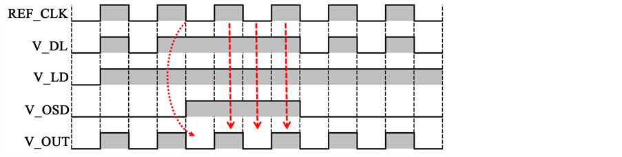
Figure 4. Proposed SE-ECC error correction process.
Table 1. SE-ECC truth table.
and area complexity is high reduced in comparison with [3] . Furthermore, it can simultaneously mitigate the missing pulse without affecting the locked state of DLL (No change in the control voltage), in this manner the SE-ECC can bolster the stability and reliability of the DLL.
3. Simulation Results
The high-energy particles that pass through critical regions of the device PN junctions, depositing energy in the silicon cause single event transients. The dense track of electron-hole pairs generated by the energy deposited by the ion strike, which move across the junction, leading to a transient current pulse on the struck node [6] . The current generated by the incident ion is modeled using a current source and injected in the strike node. This radiation strike is characterized by two collection phases: a first phase of E-field accelerated free carrier motion (fast drift current) followed by a second phase of charge collection which produces a slow current diffusion due to the free carrier density gradients .Since the E-field is present in the space charge region for an off transistor the most sensitive region to an ion strike is the drain terminal [7] . Subsequently it ably collects any charge generated in the vicinity. Double-exponential pulse is a broadly accepted shape for the SET current source [8] [9] :
 (1)
(1)
where Q is the injected charge, and τf, τr are the fall and rise time constants of the current generated by the ion. The ion-induced Single Event (SE) current profiles for linear energy transfer values between 20 MeV-cm2/mg and 100 MeV-cm2/mg for 180 nm NMOS are simulated using TCAD simulator .The NMOS transistors worst case current pulse profile for a heavy ion strike ranging over LET of 80 MeV-cm2/mg is obtained from TCAD mixed-mode simulations using ISE-TCAD [Sentaurus] is shown in Figure 5. The NMOS transistors model were calibrated for voltage over a range of 0 to 1.8 V to replicate the electrical DC transistor characteristics as defined in the PDK within a 5% error margin.
The SE-ECC was designed in 180 nm Bulk CMOS process design kits (PDKs), and simulated at frequencies between 500 MHz and 1 GHz. The circuits was simulated using ion-induced SE current profiles, obtained from the from TCAD simulations similar to ISDE bias dependent current model generator [10] , with simulated LET values between 10 MeV-cm2 mg and 100 MeV-cm2∙mg. The same type of simulation approach is proven to be effective via the experimental validation of the SET responses of mixed-signal circuits such as digital PLLs [10] . The transient responses of the outputs V_DL and V_OUT are compared. Figure 6 represents the case where

Figure 5. Ion induced current vs. time for a LET 80 MeV-cm2/mg.

Figure 6. Worst case SET response (in terms of missing pulses and phase error) generated by VCDL and SE-ECC at LET = 100 MeV-cm2/mg.
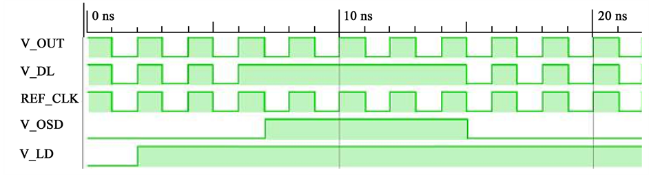
Figure 7. Worst case SET response functional simulation on a FPGA.

Figure 8. Experimental results of the SE-ECC implemented on the Artix 7 FPGA.
V_DL is perturbed and six missing pulses are generated. However, no missing pulses are observed at the DLL output V_OUT, and therefore no errors are propagated into the clock system. One can observe duty cycle variation caused by pulse skew following the switching operation of the MUX. The duty cycle variation was minimized to 5% in comparison with [3] .
The SE-ECC effectiveness is validated experimentally using a Xilinx Artix 7 implemented on a Basys3 board. The ion strikes were emulated and missing pulses errors are generated. Then the generated errors are injected in to the SE-ECC, Figure 7 shows the functional simulation of the SE-ECC. The experimental results of SE-ECC are obtained and analysed using ChipScope Pro Analyzer tool, the SET response on SE-ECC on injected missing pulses are shown in Figure 8. These results conclude the portability and robustness of SE-ECC.
4. Conclusion
A SE-ECC was implemented in a 180 nm CMOS process and measured the accuracy of mitigation on simulations at LETs up to 100 MeV-cm2/mg. The error correction technique completely eliminates missing pulses, independent of the technology node or the operating frequency of the DLL, as proven by simulation and emulation results and also any strike within the error correction circuit itself will have no significant impact on the DLL output signal. This SEH technique can be applied to a variety clock circuit using single or differential output cell topologies.
Cite this paper
S. Balaji,S. Ramasamy, (2016) Error Correction Circuit for Single-Event Hardening of Delay Locked Loops. Circuits and Systems,07,2437-2442. doi: 10.4236/cs.2016.79210
References
- 1. Maillard, P., Holman, W.T., Loveless, T.D., Bhuva, B.L. and Massengill, L.W. (2010) An RHBD Technique to Mitigate Missing Pulses in Delay Locked Loops. IEEE Transactions on Nuclear Science, 57, 3634-3639.
http://dx.doi.org/10.1109/tns.2010.2087357 - 2. Sengupta, R., Vermeire, B., Clark, L.T. and Bakkaloglu, B. (2010) A 133 MHz Radiation-Hardened Delay-Locked Loop. IEEE Transactions on Nuclear Science, 57, 3626-3633.
http://dx.doi.org/10.1109/tns.2010.2086485 - 3. Maillard, P., Holman, W.T., Loveless, T.D. and Massengill, L.W. (2013) A New Error Correction Circuit for Delay Locked Loops. IEEE Transactions on Nuclear Science, 60, 4387-4393.
http://dx.doi.org/10.1109/tns.2013.2288103 - 4. Stojcev, M. and Jovanovic, G. (2008) Clock Aligner Based on Delay Locked Loop with Double Edge Synchronization. Microelectronics Reliability, 48, 158-166.
http://dx.doi.org/10.1016/j.microrel.2007.02.025 - 5. Kao, S.-K., Chen, B.-J. and Liu, S.-I. (2007) A 62.5-625-Mhz Anti-Reset All-Digital Delay-Locked Loop. IEEE Transactions on Circuits and Systems II: Express Briefs, 54, 566-570.
http://dx.doi.org/10.1109/tcsii.2007.895326 - 6. Adell, P., Schrimpf, R. D., Barnaby, H. J., Marec, R., Chatry, C., Calvel, P., Barillot, C. and Mion, O. (2000) Analysis of Single-Event Transients in Analog Circuits. IEEE Transactions on Nuclear Science, 47, 2616-2623.
http://dx.doi.org/10.1109/23.903817 - 7. Naseer, R., Boulghassoul, Y., Draper, J., DasGupta, S. and Witulski, A. (2007) Critical Charge Characterization for Soft Error Rate Modeling in 90nm SRAM. Proceeding of IEEE International Symposium on Circuits and Systems (ISCAS), New Orleans, 27-30 May 2007, 1879-1882.
- 8. Messenger, G.C. (1982) Collection of Charge on Junction Nodes from Ion Tracks. IEEE Transactions on Nuclear Science, 29, 2024-2031.
http://dx.doi.org/10.1109/tns.1982.4336490 - 9. Wirth, G.I., Vieira, M.G., Neto, E.H. and Kastensmidt, F.L. (2008) Modeling the Sensitivity of CMOS Circuits to Radiation Induced Single Event Transients. Microelectronics Reliability, 48, 29-36.
http://dx.doi.org/10.1016/j.microrel.2007.01.085 - 10. Loveless, T.D., Massengill, L.W., Bhuva, B.L., Holman, W.T., Casey, M.C., Reed, R.A. and Melinger, J.S. (2008) A Probabilistic Analysis Technique Applied to a Radiation-Hardened-by-Design Voltage-Controlled Oscillator for Mixed- Signal Phase-Locked Loops. IEEE Transactions on Nuclear Science, 55, 3447-3455.
http://dx.doi.org/10.1109/tns.2008.2005677