Journal of Modern Physics
Vol.3 No.9(2012), Article ID:22642,5 pages DOI:10.4236/jmp.2012.39132
Nanocapacitor with a Cantor Multi-Layered Structure
1Department of Electronics, Systems and Informatics, Western Institute of Technology and Higher Education, Periferico Sur Manuel Gomez Morin, Tlaquepaque, Mexico
2Department of Mathematics and Physics, Western Institute of Technology and Higher Education, Periferico Sur Manuel Gomez Morin, Tlaquepaque, Mexico
Email: gabrielglez@iteso.mx
Received July 6, 2012; revised August 10, 2012; accepted August 17, 2012
Keywords: Nanocapacitor; Cantor Structure; Schrödinger-Poisson Equation
ABSTRACT
We calculate numerically the quantum capacitance of a nanocapacitor formed of oxide-silicon layers deposited alternately with their widths following a Cantor set structure. We show that this configuration brings about a nano-hybrid capacitor which allows a classical and quantum behavior depending on the Cantor generation. In addition, we propose an approximate equivalent circuit representation for the nano-hybrid capacitor.
1. Introduction
In recent years the storage of big energy quantities has become a vital work all over the world. The conventional batteries can store big quantities of energy, but the time of charge is much longer than the performance in a capacitor, so that lead us to one solution, capacitors with high energy storage. Electrical energy storage devices fall into three categories. Batteries, which store large amounts of energy but cannot provide high power or fast recharge. Electrochemical capacitors (ECCs), also relying on electrochemical phenomena, offer higher power at the price of relatively lower energy density. Electrostatic capacitors (ESCs), which store charge on the surfaces of two metallic conductors. This makes them capable of high power and fast recharge, but at the price of lower energy density.
Recent advances in nanotechnology have shown that nanocapacitors that make use of densely packed interfaces and thin films have the potential to serve as the basis of next generation energy systems. One approach to making such devices is to build multilayer structures of large area inside the open volume of a nanostructured template by using atomic layer deposition techniques. It should be possible to scale devices fabricated with this approach to make viable energy storage systems that provide both high energy density and high power density [1].
The nanocapacitor structure analyzed in this article is formed of oxide-silicon layers deposited alternately with their widths following a Cantor set structure. The use of highly regular nanostructures promises both high energy and high power density. In recent years the study of fractals has attracted much attention because many physical phenomena, natural structures and statistical processes can be analysed and described by using a fractal approach [2,3]. From a mathematical point of view, fractals are self-similar structures obtained by performing a basic operation, called a generator, on a given geometrical object called an initiator, and repeating this process on multiple levels; in each one of them, an object composed of sub-units of itself is created that resembles the structure of the whole object (See Figure 1). Mathematically, this property should hold on all scales. However, in the real world, there are necessarily lower and upper bounds over which such self-similar behavior applies. The simplest fractal is the Cantor set, shown in Figure 1, which can be obtained by means of an iterative construction. The first step (S = 0) is to take a segment of unit length (layer of SiO2). The next one (S = 1) is to divide the segment into three equal parts of length 1/3 and remove the central one (we just add a layer of Si in the center). This process is continued indefinitely.
In this article, a self consistent one-dimensional solution of the Schrödinger-Poisson equation [4-6] is used to obtain the electron distribution and capacitance in a nanocapacitor with a Cantor multilayer structure. In addition, we propose an approximate equivalent circuit representation for the nanocapacitor which mimics the increase of capacitance due to quantum effects. The article is organized as follows. First we will start by giving the physical and mathematical model of the problem and the basic relations of the theory. Then we will analyze the results and propose an equivalent circuit for the nanocapacitor. The conclusions are summarized in the last section.
2. Physical and Mathematical Model
We can model the nanocapacitor by setting up a lattice along the z-direction with the channel sandwiched between two insulators (see Figure 2). Where t1 and t2 are the nearest neighbors effective couplings and a is the lattice parameter. Ecnox and Ecsi are the SiO2 and Si electrochemical potentials of 9 eV and 1.12 eV [7,8], respectively. This model brings about a tight-binding Hamiltonian [9] which in matrix form reads for the case of 8 atoms and the first Cantor generation as: (see Equation (1)).
The most commonly used technique to obtain the required self-consistent Schrödinger-Poisson solution is the so called relaxation method [10-12]. In this method, a trial potential distribution  is used to solve the Schrödinger equation
 (2)
(2)
and the resulting wavefunctions and the energy eigenvalues are used to calculate the charge density in the quantum well regions [10-12],
 . (3)
. (3)
The Poisson equation is then solved using this charge density to get the new potential distribution 
 (4)
(4)
For the solution of Schrödinger equation in the next iteration, a linear combination of  and
and  given by
  is used as the input potential, where f is known as the relaxation factor. The whole procedure is repeated until convergence, i.e. the input and the output potentials
  and
and  are equal within the desired accuracy [11- 13].
To obtain the capacitance of the nanocapacitor we use

Figure 1. Cantor fractal from zero to fourth generation, in our nanocapacitor proposal we replace the lines for SiO2 and the spaces for Si.
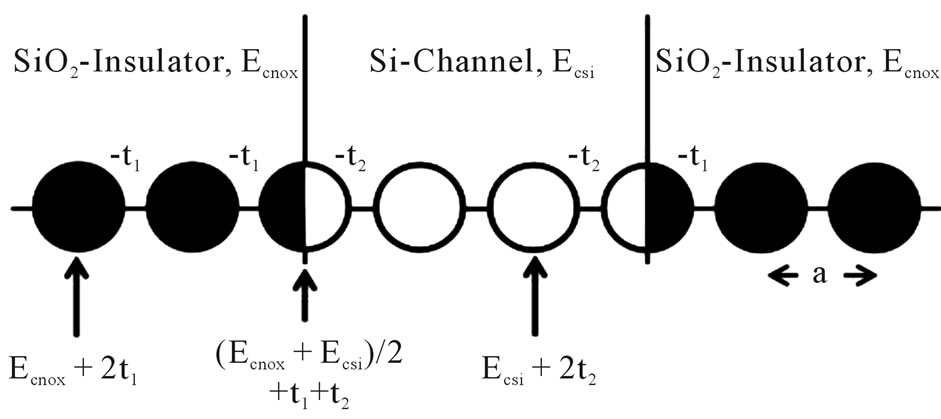
Figure 2. One-dimensional one-band effective mass Hamiltonian used in a Oxide-Silicon-Oxide device.
the relation . The change in the electrostatic charge per unit area
  for a small change in the bias across the device is given by integrating
 , i.e.
 .
.
Therefore, the capacitance is obtained through the slope of the graph  as a function of the gate voltage applied to the nanocapacitor [14,15].
3. Results
We have analyzed a nanocapacitor with oxide-silicon layers deposited alternately with their widths following a Cantor set structure using the self consistent SchrödingerPoisson equations (see Figure 3). We have chosen to work with a one dimensional chain of 80 atoms with a lattice parameter of  everywhere in order to have three Cantor generations and the total length of the chain be less than 100 nm. The zeroth Cantor generation is given by the classical parallel plate capacitor with SiO2 in between the parallel plates. The next Cantor generation has a Si layer sandwiched between two insulators, i.e. each layer in this Cantor generation is composed of 26
 (1)
(1)
 (a)
(a) (b)
(b) (c)
(c) (d)
(d)
Figure 3. The graph shows our nanocapacitor and classical circuit for the (a) zeroth Cantor generation; (b) first Cantor generation; (c) second Cantor generation; (d) third Cantor generation.
atoms which gives a total of 78 atoms and 2 atoms have been taken as interfaces between layers according to our physical model (see Figure 2). This process is repeated two more times to construct the second and third Cantor generations respectively (see Figure 3).
Figure 4 shows the electron density for the dimensional chain of 80 atoms with a third Cantor generation multilayer structure.
We used  and
and  as tunneling amplitudes between atoms, with effective silicon and silicon-dioxide mass of
  and
and 
 respectively. We used a relative dielectric constant for silicon of
  and for silicon-dioxide of
  respectively. Also, the gate voltage is assumed to be 0.25 V.
From the electron distribution depicted in Figure 4 it is clearly shown how the size quantization effects are enhanced by decreasing the width of the channels. It is

Figure 4. Charge density for a one dimensional chain of 80 atoms.
interesting to note that we have classical and quantum charge distributions in the same nanostructure which makes our device an hybrid nanocapacitor.
In order to compare the total capacitance of the nanocapacitor and a classical capacitor we calculated first the classical capacitance as a simple series combination of classical capacitors for each Cantor generation using the following simple expression
 (5)
(5)
The Cantor fractal structure sets a special model for the total capacitance since the distance of the insulator decreases  for each generation. The total capacitance per unit area for the zeroth Cantor generation is given by
 (6)
(6)
with  and
and . Based on this initial value, we construct the first order Cantor generation by inserting Silicon at the middle of the nanostructure (Figure 3(b)), the total capacitance will be equal to two capacitors in series with capacitance three times bigger than C0, due to the width reduction i.e.
 (7)
(7)
The next Cantor generation will have four capacitors (Figure 3(c)), with capacitance nine times bigger than C0 as shown on Figure 3.
 (8)
(8)
Following this logic, we can deduce a general classical formulafor the total capacitance in a Cantor serial structure:
 (9)
(9)
With Equation (9) and the value of C0, we can calculate the total capacitance for the nth Cantor generation (see Table 1).
We calculate the capacitance of the nanocapacitor by directly integrating the electron density for different bias voltages, i.e.
 (10)
(10)
The capacitance is obtained through the slope of the graph  as a function of the gate voltage applied to the nanocapacitor (see Figure 5). The values for the slopes are tabulated in Table 1. Note how the quantum capacitance, which takes into account quantum effects, is 10 times bigger than the classical capacitance for the third Cantor generation.
In order to explain the quantum capacitance with an equivalent classical circuit we must think in an hybrid quantum-classical model in a series-parallel configuration (see Figures 6-8).
For the first Cantor generation, i.e. n = 1, we have
 (11)
(11)

Table 1. Classical and quantum capacitance values from 0th to 3rd Cantor fractal generation.

Figure 5. Electron density per unit area ηS in the first, second and third order Cantor generation as a function of the gate voltage.

Figure 6. Hybrid classical-quantum circuit model for the first Cantor generation.

Figure 7. Hybrid classical-quantum circuit model for the second Cantor generation.

Figure 8. Hybrid classical-quantum circuit model for the nanocapacitor device with a Cantor multilayer structure.
From the Ec. 11 we can deduce that the quantum capacitance value is  , a very small value because the capacitance in this region of the silicon is dominated by a classical distribution.
For the second Cantor generation, we have
 (12)
(12)
Equation (12) give us a value for the quantum capacitance of .
.
For the third Cantor generation we can calculate  in the same way, i.e. finding the equivalent capacitance of the circuit given in Figure 8 and then solving for
 . The quantum capacitance for the third Cantor generation is
  . Here we can observe that the quantum capacitance dominates over the classical capacitance which enhances the energy storage of this nanocapacitor.
4. Conclusion
In summary, we have demonstrated numerically that a nanocapacitor with a Cantor multi-layered structure formed of oxide-silicon layers presents a classical and quantum behavior depending on the Cantor generation. We have shown that the total capacitance depends on the Cantor generation and increases dramatically when the quantum distribution dominates over the classical distribution. We also proposed an approximate equivalent circuit representation for the nanohybrid capacitor which mimics the behavior of the nanocapacitor.
5. Acknowledgements
David González and Ricardo Bustos would like to acknowledge financial support from ITESO. We thank Francisco Javier González for useful discussions.
REFERENCES
- D. Goldhaber-Gordon, M. S. Montemerlo, J. C. Love, G. J. Optiteck and J. Ellenbogen, “Overview of Nanoelectronic Devices,” Proceedings of the IEEE, Vol. 85, No. 4, 1997, pp. 521-540. doi:10.1109/5.573739
- B. B. Mandelbrot, “The Fractal Geometry of Nature,” Freeman, New York, 1983.
- J. A. Monsoriu, F. R. Villatoro, M. J. Marín, J. Pérez and L. Monreal, “Quantum Fractal Superlattices,” American Journal of Physics, Vol. 74, No. 9, 2006, pp. 831-836. doi:10.1119/1.2209242
- J. Sune, P. Olivo and B. Ricco, “Self-Consistent Solution of Poison and Schrdinger Equations in Accumulated SemiConductor-Insulator Interfaces,” Journal of Applied Physics, Vol. 70, No. 1, 1991, p. 337. doi:10.1063/1.350278
- S. L. Lo, D. Buchanan, Y. Taur and W. Wang, “Quantum Mechanical Modeling of Electron Tunneling Current from the Inversion Layer of Ultra-Thin Oxide nMOSFETs,” IEEE on Electron Device Letters, Vol. 18, No. 5, 1997, pp. 209-211. doi:10.1109/55.568766
- A. Ghetti, “Characterization and Modeling of the Tunneling Current in Si-SiO2-Si Structures with Ultra-Thin Oxide Layer,” Microelectronic Engineering, Vol. 59, No. 1-4, 2001, pp. 127-136. doi:10.1016/S0167-9317(01)00656-6
- R. Castagne and A. Vapaille, “Description of the SiO2-Si Interface Properties by Means of very Low Frequency MOS Capacitance Measurements,” Surface Science, Vol. 28, No. 1, 1971, pp. 157-193, doi:10.1016/0039-6028(71)90092-6
- S. H. Lo, D. A. Buchanan and Y. Taur, “Modeling and Characterization of Quantization, Polysilicon Depletion, and Direct Tunneling Effects in MOSFETs with Ultrathin Oxides,” IBM Journal of Research and Development, Vol. 43, No. 3, 1999, pp. 327-337. doi:10.1147/rd.433.0327
- A. Ghetti, J. Bude, P. Silverman, A. Hamad and H. Vaidya, “Modeling and Simulation of Tunneling Current in MOS Devices including Quantum Mechanical Effects,” IEICE Transactions on Electronics, Vol. E83-C, No. 8, 2000, pp. 1175-1182.
- P. Harrison, “Quantum Wells, Wires and Dots,” 2nd Edition, Wiley, Hoboken, 2008.
- S. Datta, “Quantum Transport: Atom to Transistor,” Cambridge University Press, Cambridge, 2005. doi:10.1017/CBO9781139164313
- D. K. Ferry and S. M. Goodnick, “Transport in Nanostructures,” Cambridge University Press, Cambridge, 2001.
- M. Y. Dogish and F. D. Ho, “A Comprehensive Analytical Model for Metal-Insulator Semiconductor (MIS) Devices,” IEEE Transactions on Electron Devices, Vol. 39, No. 12, 1992, pp. 2771-2780. doi:10.1109/16.168723
- K. S. Krisch, J. D. Bude and L. Manchanda, “Gate Capacitance Attenuation in MOS devices with Thin Dielectrics,” IEEE Electron Device Letters, Vol. 17, No. 14, 1996, pp. 521-524. doi:10.1109/55.541768
- W. Magnus, and W. Schoenmaker, “Full Quantum Mechanical Model for the Charge Distribution and the Leakage Currents in Ultra-Thin MOS Capacitors,” Journal of Applied Physics, Vol. 88, No. 10, 2000, pp. 5833-5842. doi:10.1063/1.1320025