A Parallel Circuit Simulator for Iterative Power Grids Optimization System ()
1. Introduction
With the deep submicron technologies, it has become possible to mount a large and high performance system on one VLSI chip. However, the power supply voltage is lowering along with shrinking of the device size. On the other hand, the power consumption is increasing because the number of transistors and the clock frequency increase. Therefore, IR-drop and electro-migration (EM) in the power grids make functions and devices unreliable. It becomes more serious problem than ever. The power grid optimization has become very important for ensuring the reliability, correctness and stability of the design. In recent years, many prior researches [1-6] have been proposed to solve the problem. A heavy simulation time is required to analyze the problem of heat and electromagnetic field [3]. Moreover, a high speed and high accurate circuits simulator is required for iterative optimization which includes execution of the simulation many times for its evaluation.
Thus, several hardware accelerator approaches have been reported [7-12]. Lee et al. achieved 25 times high speed processing in the timing verification using multi CPU [7]. Nakasato et al. demonstrated particle simulation by floating point arithmetic on an FPGA [8]. Watanabe et al. introduced parallel-distributed time-domain circuit simulation of power distribution networks by multiple PC [9]. However, no research of hardware accelerator to optimize power grids of VLSI has been reported.
This paper aims at estimating the performance improvement by hardware implementation of the circuit simulation in the power supply wiring. We have analyzed accuracy, speed, and hardware resources to implement typical numerical analysis algorithms of circuit simulation, in cases of floating point and fixed point variables, software and hardware. Moreover, we propose an efficient hardware circuit simulator for power grid optimization. It achieves high speed simulation by adopting pipeline and parallel processing. The proposed simulator introduces hardware-oriented fixed point arithmetic instead of floating point arithmetic. The hardware-oriented fixed point arithmetic realizes the high area-efficiency by reducing hardware resources, and it also accomplishes the high accuracy by controlling intervals of simulation.
2. Power Grid Optimization System
2.1. Power Grid Optimization Algorithm
The power grid consists of two vertical and horizontal layers. Those are interconnected by contacts at the intersection. The equivalent circuit model for proposed power grid optimization system is shown in Figure 1.
Decoupling capacitors are inserted to decrease dynamic IR-drop and inductor noise to the power grid. At each grid area, four edges of resistances are placed. The capacitance which connected to each node represents the sum of the decoupling capacitance and the wiring capacitance.
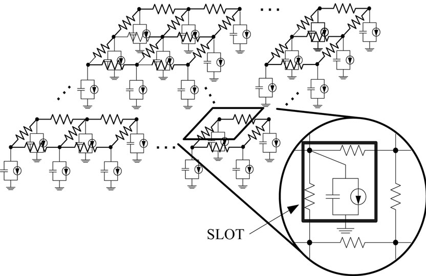
Figure 1. Equivalent circuit model for power grids.
Current source which connected to each node corresponds to the current consumption of functional block of VLSI. These circuit elements connected with a grid are defined as SLOT. The power grid optimization is defined as a multi-objective optimization problem. First objective is to reduce the risk of timing error which is caused by transient and local IR-drop. Second objective is to reduce the risk of wire break which is caused by excess of electric current density at a portion of a wiring. Third objective is to reduce the risk of failing signal wiring which is caused by local congestion of wires. We have already proposed an algorithm to solve these trade-off problems [13-15]. It defines the optimization problem by using an evaluation function which unifies the risks of multiple objectives. The optimization is scheduled by an iterative improvement. Iterative operation consists of circuit simulation, evaluation of risks, and small modification of wire width or decupling capacitance.
2.2. Organization of Power Grid Optimization System
The power grid optimization system consists of three parts, the simulation part, the evaluation part and the optimization part, as shown in Figure 2. A new repetitive optimization and evaluation function is introduced to improve the multiple physical issues [13]. To evaluate circuits, an original metrics, RISK, is defined. The proposed power grid optimization system adopts the algorithm as a base algorithm of the optimization part. Effectiveness of the power grid optimization system is determined by communication-overhead between each part, in addition to the simulation accuracy and the processing speed.
The simulation part is the most time consuming. It simulates the circuit behavior and calculates the electric current of each edge and the voltage of the each node. It takes more than 99% of the total computation time. Therefore, reduction of processing time of the simulation part is most important from the point of high speed opti-

Figure 2. Power grid optimization system.
mization processing. The evaluation part defines a risk function for each design metric, i.e., IR-drop, EM, and wiring congestion, from simulation results. IR-drop RISK is defined as a probability of causing the timing error. An increase of current density raises the EM RISK and it cause a deterioration and disconnection of wires to be unable to operate. As a result, the circuit doesn’t operate. The wiring congestion RISK represents the proportion of the wiring resource in a SLOT area. It is a restriction of preventing from an excessive wiring and state that cannot be wired. Because each grid is composed of the power grid, decoupling capacitor and signal wire, totals of those areas are compared with the grid area.
The optimization part improves IR-drop, EM and wiring congestion by changing wiring width and decoupling capacitance. Performance of the power grid optimization system is determined by communication overhead between each part, in addition to the simulation accuracy and the processing speed.
2.3. Simulation Algorithm
2.3.1. Circuit Analysis Method
This section summarizes typical numerical analysis methods which can be used for the power grid simulation. Euler method and Runge-Kutta method are typical numeric method to solve differential equations. Generally, small time step must be selected to analyze steadily by Forward Euler method (FE).
The computation algorithm is simple and needs smaller hardware resources, but it may easily diverge. RungeKutta methods require complex calculation, but the simulation is more stable even though we select a larger time step than FE. Thus, we must carefully select the numerical algorithm for the given problem. We have examined 100 or more variations of power grids and evaluated.
The test data is composed of four size variations, 50 × 50, 100 × 100, 200 × 200, 500 × 500. Also, it is composed of five RC distributions, regular, random, two types of hand-specified, extracted from real chips. The largest RC time constant was about 20 times larger than the minimum one.
As the results, the accuracy is almost same for each numerical method and we have selected FE. For the evaluation of numerical methods see the next section.
2.3.2. Evaluation of the Accuracy by Comparing with SPICE
This In order to verify the proposed algorithm’s validity, comparative experiments are performed using the following two types of circuit simulations: 1) Accuracy comparison between double-precision floating point arithmetic and SPICE; and 2) Accuracy comparison between single-precision fixed point arithmetic and double-precision floating point arithmetic. The power grid which is used for the analysis is a structure of uniform RC distribution, and R and C in the power grid were randomly set from predefined three values. The power grid scale is 10 × 10 grids. The dynamic current consumption is changed in every 10 [μsec]. In conversion into the fixed point, the fraction part of all variables was set to 22-bit. Since 32-bit adders and multipliers are used for experiment, the overflow happened in 23-bit or more.
Firstly, the result of experiments on each simulation with double-precision arithmetic is shown in Figures 3 and 4. The step size is an important point in the transition analysis, and it is necessary to set it to small step to execute an accurate analysis. The small step is set 0.63 [μsec]. The smallest RC was 20 [μsec]. All the analysis methods have been achieved high accuracy compared with SPICE.
Next, experiments on fixed point arithmetic are executed by various step sizes, and the error is verified with the floating point arithmetic. In small step size, the maximum error margin and the average error margin are shown in Tables 1 and 2.
In the uniform RC distribution, all nine patterns, the

Figure 3. Simulation result by Euler method with small step size.

Figure 4. Simulation result by Euler method with small step size.

Table 1. Error by fixed point arithmetic for uniform RC circuit.

Table 2. Error by fixed point arithmetic for random RC circuit.
combination of the wiring resistance and the capacitance, are executed. Table 2 shows the maximum error and the average error of 100 kinds of circuit selected at random. The high accurate simulation has been achieved with a small time step.
In fixed point arithmetic, fourth order Runge-Kutta Method (RK4) and Runge-Kutta marsun method (RKM) obtain a good result. In addition, the error of uniform RC distribution is larger than that of random circuit. The computational complexity of FE and Modified Euler method (ME) are small. In contrast, RK4 and RKM are complex for computation, though they can execute an accurate analysis.
In our preliminary experiments, FE and RK4 diverged on the same time step. Therefore, FE is superior to RK4 in case of the power grid optimization problem.
2.3.3. Simulation Flow
Voltage and current change in each node at small time step is analyzed based on information of the RC distribution, the current consumption distribution, and the supply voltage, etc. The simulation flow is shown in Figure 5, and a part of the equivalent circuit is shown in Figure 6.
In the simulation part, the current of each wiring is calculated from voltage distribution and the wiring resistance. Then, the charge which accumulates in the capacitance connected with each node is calculated, and the voltage is derived every small time step dT. These processing are iterated during simulation time for entire power grid Tm, and assumed to be end of simulation. To obtain the voltage at each node, the charge is changed by the inflow current Ileft and Iup, the outflow current Iright and Idown, and the current consumption Icon. Voltage and current change in each node are computed based on RC distribution at small time step.
For more high speed simulation, the simulation with hardware is effective, but the achievement of the hardware simulator is not easy according to the restriction of the error margin and the hardware resource. To examine whether it is feasible to make the present simulation hardware, the accuracy of the analysis by the doubleprecision floating point arithmetic and by the single-precision fixed point arithmetic are verified. The error margin is caused by replacing with fixed point arithmetic. It is because the fixed point arithmetic can be processed at the same speed as the integer operation. Additionally, the area of the fixed point arithmetic unit is far smaller compared with the floating point arithmetic unit.
3. Hardware Architecture for Power Grid Simulation
The proposed simulation algorithm adopts fixed point arithmetic. It achieves the same processing speed as the integer operation, and has an advantage of area-efficiency when implementing on hardware. Fixed point arithmetic includes a risk of overflow; however, this risk is reduced by correction processing and bit shift. The simulation part computes the voltage and the current of each node of power grid, and stores the simulation results into memory. Furthermore, it is necessary to control the simulation and the memory behavior to achieve high speed simulation. Figure 7 shows the block diagram of the power grid simulation which corresponds to simulation module and memory access as shown in Figure 2. Control module controls state transition and timing of each module. Each circuit variables are stored in each memory. Wiring resistance and capacitance are updated when changing the circuit design.
The voltage and the charge are updated whenever advancing at a small time step. Therefore, these are stored in RAM. Circuit variables are fetched from the memory into the simulation module, and the results are written into memory.
The simulation module is composed by adder, subtractor, and multiplier, and doesn’t use divider. Current is calculated by dividing potential difference of wiring resistance, however divider needs a lot of implementation areas. Therefore, divider is converted into multiplier by storing each reciprocal when wiring resistance and capacitance are stored in the memory. Figure 8 shows the calculation procedure in the simulation module.
Input variables, “Gright”, “Gdown” and “Z” show the reciprocal of wiring resistance and capacitance respectively. In the current calculation of the hardware algorithm, only outflow current is computed as shown in Figure 4. Because inflow current of a point corresponds to outflow current of the adjacent point (left side or upper side).

Figure 7. Block diagram of the power grid simulation.
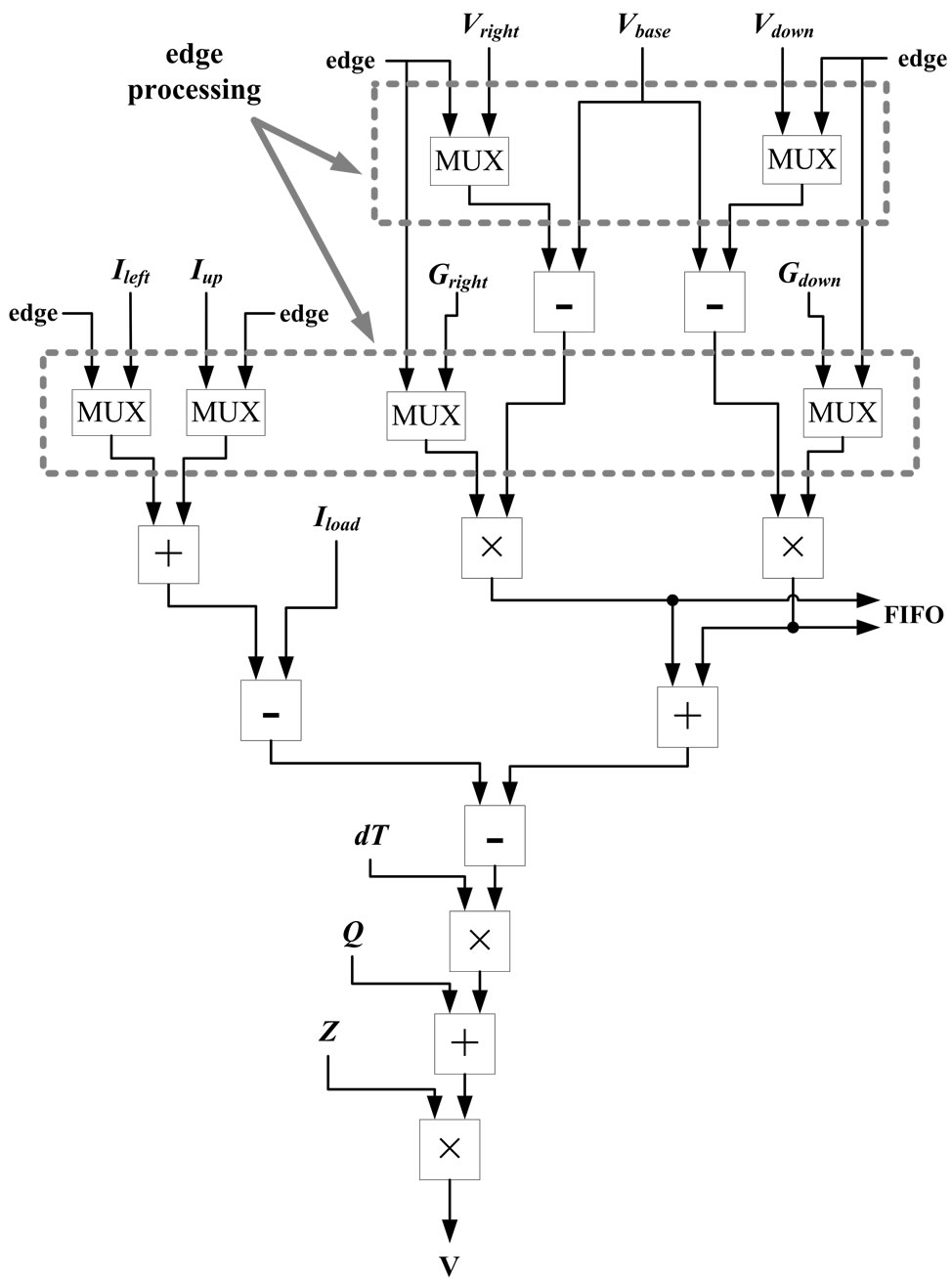
Figure 8. Calculation procedure in the simulation module.
The simulation module processes the circuit variables from memory, and writes simulation result into the memory. The variables written in the memory are the current, the charge, and the voltage. The current is used to calculate the RISK, the charge is necessary for each grid simulation, and the voltage is both. When the edge of the power grid is simulated, the variable is switched to the exception parameter by multiplexer (MUX) because the adjacent SLOT doesn’t exist.
4. Hardware Algorithm
4.1. Pipeline Processing
Registers are inserting between each arithmetic unit to achieve pipeline processing. The proposed pipeline processing is composed of eight stages, and the data of each SLOT is transferred to the simulation module per clock cycle. The simulation flow by pipeline processing is as follows.
1) Each variable is stored from the memory to register.
2) Calculation of potential difference.
3) Calculation of each current.
4) Addition of each current (Iright, Idown, Ileft and Iup).
5) Addition of Stage 4 and current source.
6) Calculation of inflow/outflow currents in small time step.
7) Computation of charge.
8) Computation of voltage.
Figure 9 shows the pipeline stage in the simulation module. All nodes of the power grid are sequentially simulated in the simulation module.
Because current calculation of a node require the voltage of the adjacent node, it is necessary to wait until the adjacent node finishes simulating, even if the node finishes simulating. Horizontal size and vertical size of power grid are defined as H_SIZE and V_SIZE. In an ideal pipeline processing, H_SIZE times V_SIZE clocks are needed for the simulation of all nodes. Moreover, 8 + H_SIZE clocks are needed to finish eight stage pipeline processing of a node and the adjacent node.
4.2. Parallel Processing
Figure 10 shows an example of which a circuit is divided